Description
www.DataSheet4U.com K7R323682C K7R321882C K7R320982C 1Mx36 & 2Mx18 & 4Mx9 QDRTM II b2 SRAM 36Mb QDRII SRAM Specification 165 FBGA with Pb & Pb-Free.
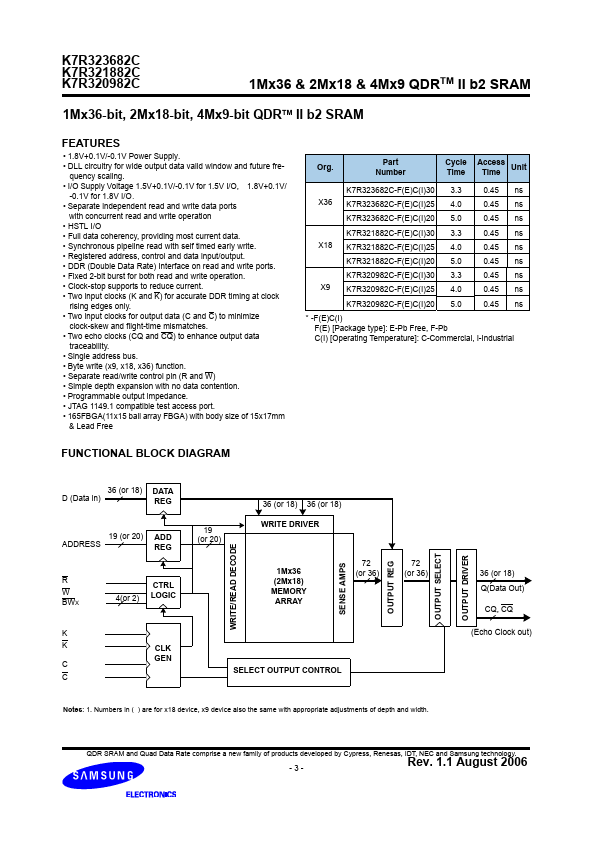
Input Clock Input Clock for Output Data Output Echo Clock DLL Disable when low Address Inputs Data Inputs 1 NOTE
Q0-35 W R BW0, BW1,BW2, BW3 VREF ZQ.
Features
* 1.8V+0.1V/-0.1V Power Supply.
* DLL circuitry for wide output data valid window and future frequency scaling.
* I/O Supply Voltage 1.5V+0.1V/-0.1V for 1.5V I/O, 1.8V+0.1V/ -0.1V for 1.8V I/O.
* Separate independent read and write data ports with concurrent read and
Applications
* where Product failure could result in loss of life or personal or physical harm, or any military or defense application, or any governmental procurement to which special terms or provisions may apply.
* Samsung Electronics reserves the right to change products or specification without notice.