Datasheet Details
- Part number
- K7R323684M
- Manufacturer
- Samsung semiconductor
- File Size
- 202.00 KB
- Datasheet
- K7R323684M_Samsungsemiconductor.pdf
- Description
- 1M x 36 & 2M x 18 QDR II b4 SRAM
K7R323684M Description
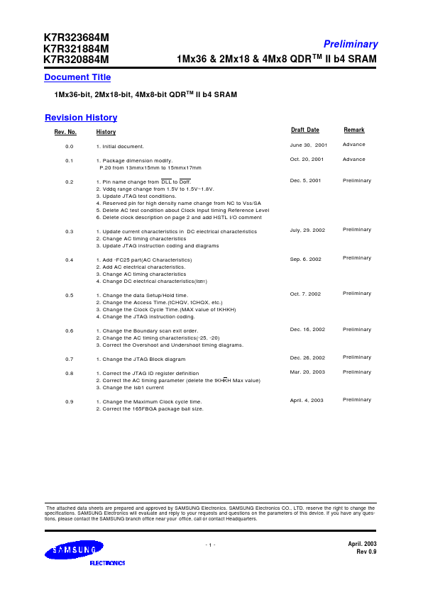
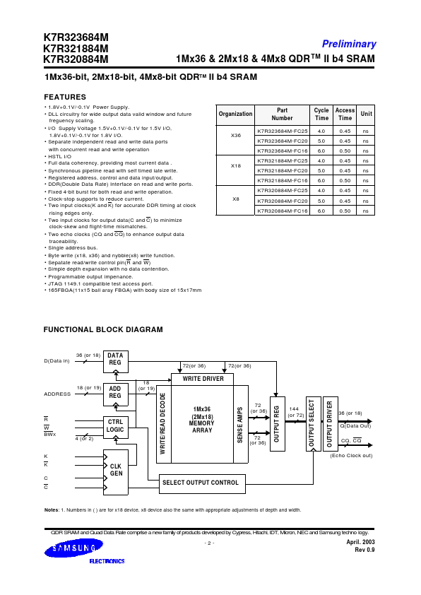
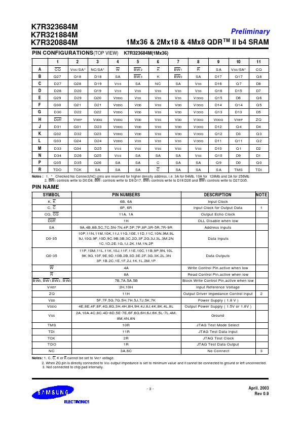
K7R323684M K7R321884M K7R320884M Preliminary 1Mx36 & 2Mx18 & 4Mx8 QDRTM II b4 SRAM Document Title 1Mx36-bit, 2Mx18-bit, 4Mx8-bit QDRTM II b4 SRAM .
on page 2 and add HSTL I/O comment
0.
📁 Related Datasheet
📌 All Tags