Datasheet Details
| Part number | K7R641882M |
|---|---|
| Manufacturer | Samsung semiconductor |
| File Size | 364.61 KB |
| Description | 2Mx36 & 4Mx18 & 8Mx9 QDRTM II b2 SRAM |
| Datasheet |
 K7R641882M_Samsungsemiconductor.pdf K7R641882M_Samsungsemiconductor.pdf
|
| Part number | K7R641882M |
|---|---|
| Manufacturer | Samsung semiconductor |
| File Size | 364.61 KB |
| Description | 2Mx36 & 4Mx18 & 8Mx9 QDRTM II b2 SRAM |
| Datasheet |
K7R641882M_Samsungsemiconductor.pdf
|
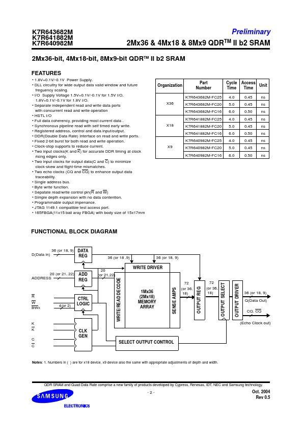
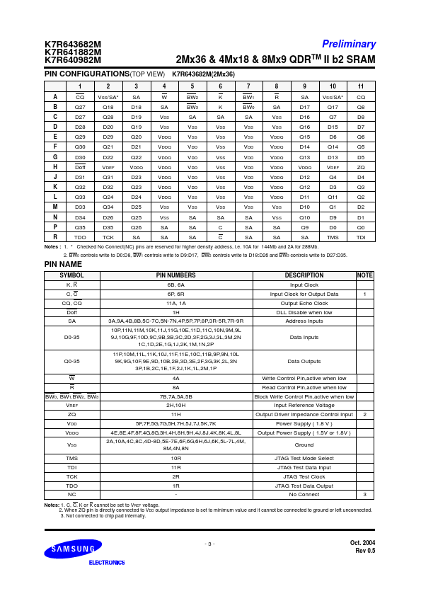
Input Clock Input Clock for Output Data Output Echo Clock DLL Disable when low Address Inputs Data Inputs 1 NOTE Q0-35 W R BW0, BW1,BW2, BW3 VREF ZQ VDD VDDQ VSS TMS TDI TCK TDO NC Data Outputs Write Control Pin,active when low Read Control Pin,active when low Block Write Control Pin,active when low Input Reference Voltage Output Driver Impedance Control Input Power Supply ( 1.8 V ) Output Power Supply ( 1.5V or 1.8V ) Ground JTAG Test Mode Select JTAG Test Data Input JTAG Test Clock JTAG Test
📁 K7R641882M Similar Datasheet