Datasheet Details
- Part number
- M470L3224FU0
- Manufacturer
- Samsung semiconductor
- File Size
- 264.46 KB
- Datasheet
- M470L3224FU0_Samsungsemiconductor.pdf
- Description
- DDR SDRAM SODIMM
M470L3224FU0 Description
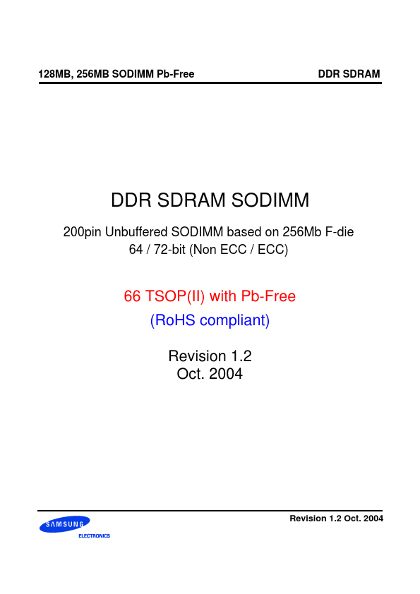
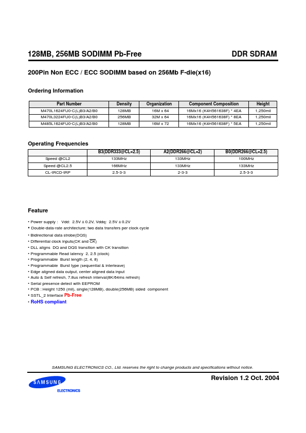
128MB, 256MB SODIMM Pb-Free DDR SDRAM DDR SDRAM SODIMM 200pin Unbuffered SODIMM based on 256Mb F-die 64 / 72-bit (Non ECC / ECC) 66 TSOP(II) with P.
Pin Name A0 ~ A12 BA0 ~ BA1 DQ0 ~ DQ63 DQS0 ~ DQS8 CK0,CK0 ~ CK2, CK2 CKE0~CKE1 CS0~CS1 RAS CAS WE CB0 ~ CB7 Function Address input (Multiplexed) Bank.
M470L3224FU0 Features
* REF VSS
D0 - D4 D0 - D4
Notes: 1. DQ-to-I/O wiring is shown as recommended but may be changed. 2. DQ
📁 Related Datasheet
📌 All Tags