Description
Input Clock Q Valid output Output Echo Clock DLL Disable Address Inputs Data Inputs NOTE
Q0-35 W R BW0, BW1,BW2, BW3 VREF ZQ VDD VDDQ VSS TMS TDI TCK TDO NC
Notes:
Data Outputs Write Control Pin,active when low Read Control Pin,active when low Block Write Control Pin,active when low Input Reference Voltage Output Driver Impedance Control Input Power Supply ( 1.8 V ) Output Power Supply ( 1.5V ) Ground JTAG Test Mode Select JTAG Test Data Input JTAG Test Clock JTAG Test Data Output No Connect 2
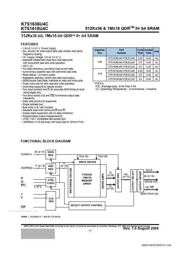
Features
- 1.8V+0.1V/-0.1V Power Supply.
- DLL circuitry for wide output data valid window and future freguency scaling.
- I/O Supply Voltage 1.5V+0.1V/-0.1V.
- Separate independent read and write data ports with concurrent read and write operation.
- HSTL I/O.
- Full data coherency, providing most current data.
- Synchronous pipeline read with self timed late write.
- Read latency : 2.5 clock cycles.
- Registered address, control and d.
 K7S1618U4C_Samsungsemiconductor.pdf