Datasheet Details
| Part number | LE25FS406 |
|---|---|
| Manufacturer | Sanyo Semicon Device |
| File Size | 278.75 KB |
| Description | 4M-bit (512K X 8) Serial Flash Memory |
| Datasheet |
 LE25FS406 Datasheet LE25FS406 Datasheet
|
|
|
| Part number | LE25FS406 |
|---|---|
| Manufacturer | Sanyo Semicon Device |
| File Size | 278.75 KB |
| Description | 4M-bit (512K X 8) Serial Flash Memory |
| Datasheet |
LE25FS406 Datasheet
|
|
|
|
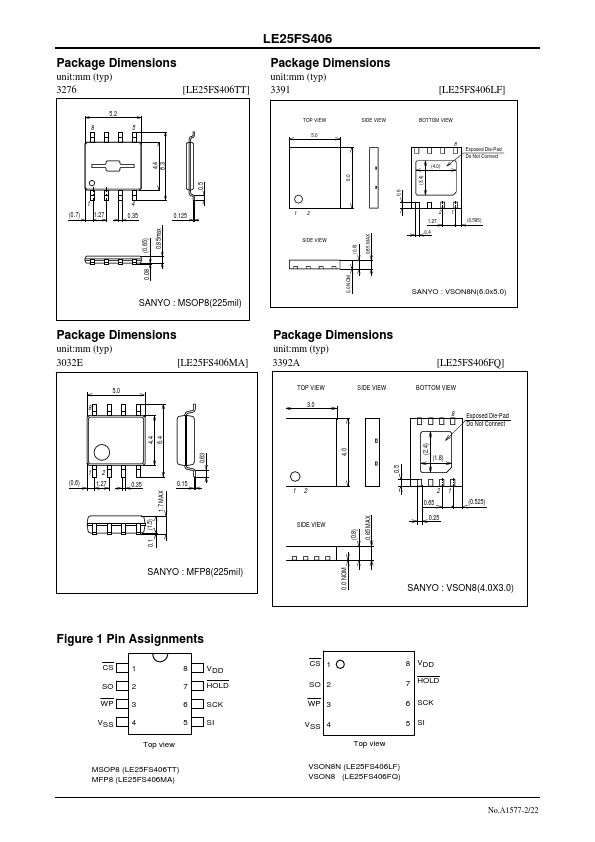
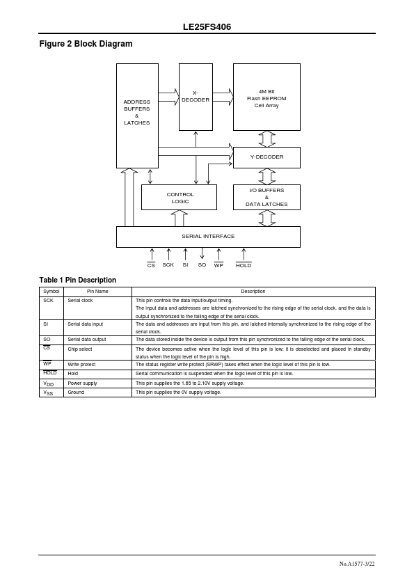
Symbol SCK Pin Name Serial clock This pin controls the data input/output timing.
📁 Similar Datasheet