LE25FW403A - 4M-bit Serial Flash Memory 30MHz SPI Bus
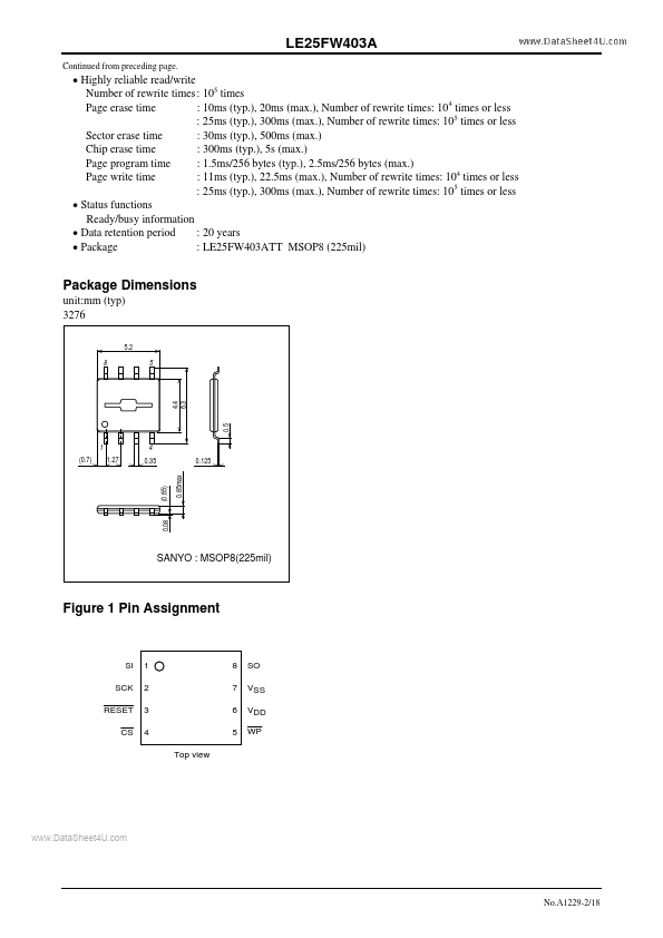
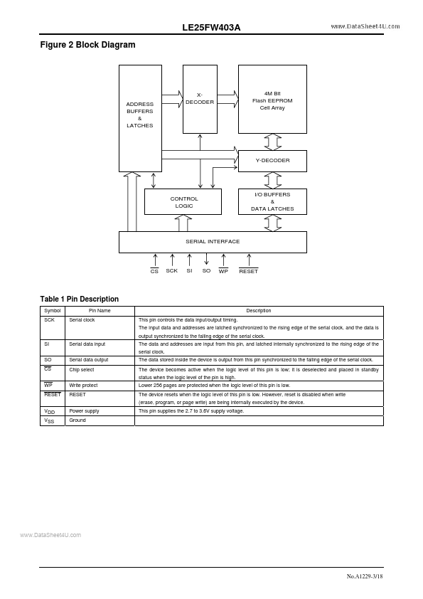
Symbol SCK Pin Name Serial clock This pin controls the data input/output timing.
The input data and addresses are latched synchronized to the rising edge of the serial clock, and the data is output synchronized to the falling edge of the serial clock.
SI SO CS WP RESET VDD VSS Serial data input Seri
Ordering number : EN A1229A CMOS IC LE25FW403A Overview 4M-bit (512K×8) Serial Flash Memory 30MHz SPI Bus The LE25FW403A is an onboard programmable flash memory device with a 512K×8-bit configuration.
It uses a single 3.0V power supply and supports the serial interface.
It has three erase functions depending on the size of memory area in which the data is to be erased: the chip erase function, the sector (64K bytes) erase function, and a page (256 bytes) erase function.
A page program me
LE25FW403A Features
* Read/write operations enabled by single 3.0V power supply: 2.7 to 3.6V supply voltage range
* Operating frequency : 30MHz
* Temperature range : 0 to 70°C
* Serial interface : SPI mode 0, mode 3 supported
* Sector size : 256 bytes/page sector, 64K bytes/secto