CY2SSTV850
Overview
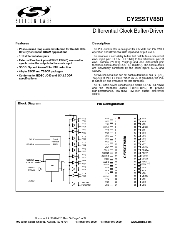
This PLL clock buffer is designed for 2.5 VDD and 2.5 AVDD operation and differential data input and output levels. This device is a zero-delay buffer that distributes a differential clock input pair (CLKINT, CLKINC) to ten differential pair of clock outputs (YT[0:9], YC[0:9]) and one differential pair feedback clock output (FBOUTT, FBOUTC).
- Phase-locked loop clock distribution for Double Data Rate Synchronous DRAM applications
- 1:10 differential outputs
- External Feedback pins (FBINT, FBINC) are used to synchronize the outputs to the clock input
- SSCG: Spread Aware™ for EMI reduction
- 48-pin SSOP and TSSOP packages
- Conforms to JEDEC JC40 and JC42.5 DDR