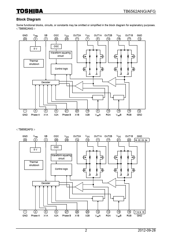
Description
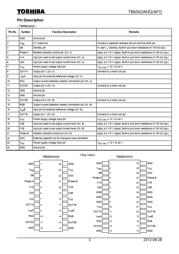
< TB6562ANG >
Pin No.Symbol
Function Description
Remarks
1
GND
Ground pin
2
Vreg
5 V output pin
3
SB
Standby pin
Connect a capacitor between this pin and the GND pin.H: start, L: Standby, Built-in pull down resistance of 100 kΩ (typ.)
4
Phase A Rotation direction control pin (Ch.A)
Apply a 0 V/5 V signal, Built-in pull down resistance of 100 kΩ (typ.)
5
X1A
Input pin used to set output current level (Ch.A)
Apply a 0 V/5 V signal, Built-in pull down resistance of 100 kΩ (ty
Features
- 2-phase/1.
- 2-phase/W 1.
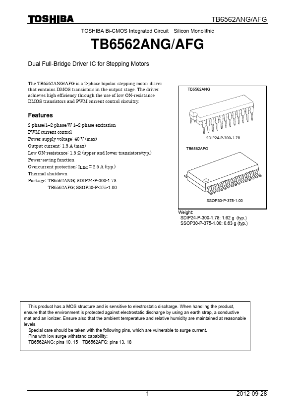
- 2-phase excitation PWM current control Power supply voltage: 40 V (max) Output current: 1.5 A (max) Low ON-resistance: 1.5 Ω (upper and lower transistors/typ. ) Power-saving function Overcurrent protection: ILIM = 2.5 A (typ. ) Thermal shutdown Package: TB6562ANG; SDIP24-P-300-1.78
TB6562AFG; SSOP30-P-375-1.00
TB6562ANG
TB6562AFG
SSOP30-P-375-1.00
Weight: SDIP24-P-300-1.78: 1.62 g (typ. ) SSOP30-P-375-1.00: 0.63 g (typ. )
This product has a MOS structure and i.
 TB6562ANG_ToshibaSemiconductor.pdf