Datasheet Details
| Part number | 74HCT107-Q100 |
|---|---|
| Manufacturer | nexperia |
| File Size | 254.58 KB |
| Description | Dual JK flip-flop |
| Datasheet |
 74HCT107-Q100 Datasheet 74HCT107-Q100 Datasheet
|
|
|
This page provides the datasheet information for the 74HCT107-Q100, a member of the 74HC107-Q100 Dual JK flip-flop family.
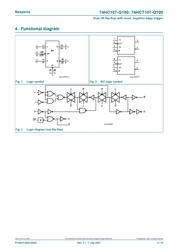
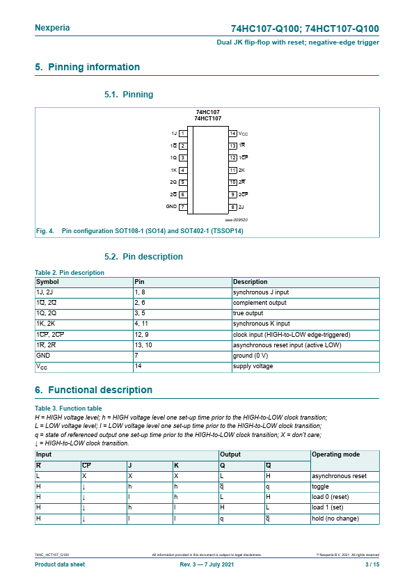
The 74HC107-Q100; 74HCT107-Q100 is a dual negative edge triggered JK flip-flop featuring individual J and K inputs, clock (CP) and reset (R) inputs and complementary Q and Q outputs.
The reset is an asynchronous active LOW input and operates independently of the clock input.
| Part number | 74HCT107-Q100 |
|---|---|
| Manufacturer | nexperia |
| File Size | 254.58 KB |
| Description | Dual JK flip-flop |
| Datasheet |
74HCT107-Q100 Datasheet
|
|
|
|