ACE4953B
ACE4953B is Dual P-Channel Enhancement Mode Field Effect Transistor manufactured by ACE Technology.
Dual P-Channel Enhancement Mode Field Effect Transistor
Description The ACE4953B uses advanced trench technology to provide excellent RDS(ON), and ultra-low low gate charge. This device is suitable for use as a load switch or in PWM applications.
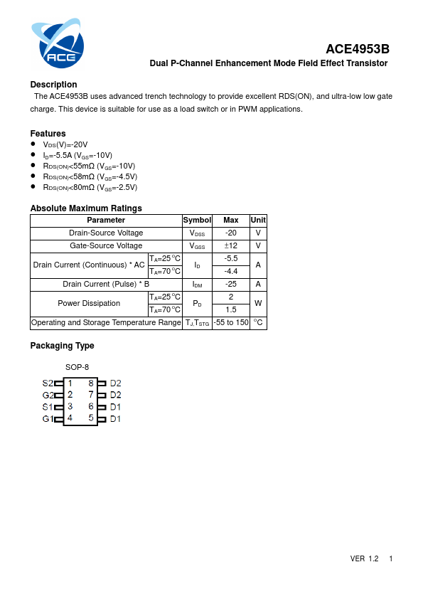
Features
- VDS(V)=-20V
- ID=-5.5A (VGS=-10V)
- RDS(ON)<55mΩ (VGS=-10V)
- RDS(ON)<58mΩ (VGS=-4.5V)
- RDS(ON)<80mΩ...