AWT6309
AWT6309 is LINEAR POWER AMPLIFIER manufactured by ANADIGICS.
FEATURES
- In Ga P HBT Technology
- High Efficiency: 40 % @ +28 d Bm output 22 % @ +17 d Bm output
- Low Quiescent Current: 15 m A
- Low Leakage Current in Shutdown Mode: <1 µA
- Internal Voltage Regulation
- Optimized for a 50 Ω System
- Low Profile Miniature Surface Mount Package: 1 mm
- CDMA 1XRTT, 1x EV-DO pliant
- Pinout Enables Easy Phone Board Migration From 4 mm x 4 mm Package
- Ro HS-pliant Package, 250 o C MSL-3
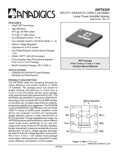
M9 Package 8 Pin 3 mm x 3 mm x 1 mm Surface Mount Module
APPLICATIONS
- CDMA/EVDO AWS/KPCS band Wireless Handsets and Data Devices The AWT6309 meets the increasing demands for higher efficiency and smaller footprint in CDMA 1X handsets. The package pinout was chosen to enable handset manufacturers to switch from a 4 mm x 4 mm PA module with few layout changes while reducing board area requirements by 44%. The AWT6309 uses ANADIGICS’ exclusive In Ga P-Plus™ technology, which bines HBT and p HEMT devices on the same die, to enable state-of-the-art reliability, temperature stability, and ruggedness. The AWT6309 is part of ANADIGICS’ High-Efficiency-at-Low-Power (HELP™) family of CDMA power amplifiers, which deliver low quiescent currents and significantly greater efficiency without a costly external DAC or .. DC-DC converter. Through selectable bias modes, the AWT6309 achieves optimal efficiency across different output power levels, specifically at low- and midrange power levels where the PA typically operates, thereby dramatically increasing handset talk-time and standby-time. Its built-in voltage regulator eliminates the need for external voltage regulation ponents. The 3 mm x 3 mm x 1 mm surface mount package incorporates matching networks optimized for output power, efficiency, and linearity in a 50 Ω system.
05/2009
PRODUCT DESCRIPTION
Figure 1: Block Diagram
Figure 2: Pinout (X-ray Top View) Table 1: Pin Description
PIN 1 2 3 4 5 6 7 8 NAME VBATT RFIN VMODE VEN GND GND RFOUT VCC DESCRIPTION
Battery Voltage RF Input Mode...