AWT6310R
AWT6310R is LINEAR POWER AMPLIFIER manufactured by ANADIGICS.
FEATURES
- -
- -
- -
- -
- Single Mode Operation: POUT ≤ +28 d Bm High Efficiency: 54 % AMPS, 39 % CDMA Low Quiescent Current: 50 m A 25 % Package Size Reduction mon VMODE Control Line Simplified VCC Bus PCB routing Reduced External ponent Count Low Profile Surface Mount Package: 1.1 mm Ro HS pliant Package, 250 o C MSL-3
AW T
0R
APPLICATIONS
- Dual-band Cellular/PCS CDMA Wireless Handsets
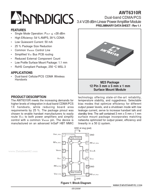
M23 Package 12 Pin 3 mm x 5 mm x 1 mm Surface Mount Module PRODUCT DESCRIPTION
The AWT6310R meets the increasing demands for higher levels of integration in dual-band CDMA/PCS 1X handsets, while reducing board area requirements by 25 %. The package pinout was chosen to enable handset manufacturers to easily route VCC to both power amplifiers and simplify control with a mon VMODE pin. The device is manufactured on an advanced In Ga P HBT MMIC technology offering state-of-the-art reliability, temperature stability, and ruggedness. Selectable bias modes that optimize efficiency for different output power levels, and a shutdown mode with low leakage current, serve to increase handset talk and standby time. The self contained 3 mm x 5 mm x 1 mm surface mount package incorporates matching networks optimized for output power, efficiency and linearity in a 50 Ω system.
GND at slug (pad)
VREF_CELL
1 Bias Control 12 GND
RFIN_CELL
11 RFOUT_CELL
..
VMODE
10 VCC2 A
VCC1 4
VCC2
RFIN_PCS 5
Bias Control
VREF_PCS 6
RFOUT_PCS
Figure 1: Block Diagram
05/2006
GND VREF_CELL RFIN_CELL VMODE VCC1 RFIN_PCS VREF_PCS 1 2 3 4 5 6 GND
Figure 2: Pinout
12 11 10 9 8 7
GND RFOUT_CELL VCC2A VCC2 GND RFOUT_PCS
Table 1: Pin...