AWT6321
AWT6321 is LINEAR POWER AMPLIFIER manufactured by ANADIGICS.
FEATURES
APPLICATIONS
- CDMA/EVDO & Cell & PCS Dual-band Wireless Handsets and Data Devices The AWT6321 addresses the demand for increased integration in dual-band handsets for North American CDMA network deployments. The small footprint 3 mm x 5 mm x 1 mm surface mount Ro HS pliant package contains independent RF PA paths to ensure optimal performance in both frequency bands, while achieving a 25% PCB space savings pared with solutions requiring two single-band PAs. The package pinout was chosen to enable handset manufacturers to easily route VCC to both power amplifiers and simplify control with a mon V MODE pin. The device is manufactured on an advanced In Ga P HBT MMIC technology offering state-of-the-art reliability, temperature stability, and ruggedness. The AWT6321 is part of ANADIGICS’ High-Efficiency-at-Low-Power .. (HELP™) family of CDMA power amplifiers, which deliver low quiescent currents and significantly greater efficiency without a costly external DAC or DC-DC converter. Through selectable bias modes, the AWT6321 achieves optimal efficiency across different output power levels, specifically at low- and midrange power levels where the PA typically operates, thereby dramatically increasing handset talk-time and standby-time. Its built-in voltage regulator eliminates the need for external switches. The 3 mm x 5 mm x
M28 Package 14 Pin 3 mm x 5 mm x 1 mm Surface Mount Module
1 mm surface mount package incorporates matching networks optimized for output power, efficiency and linearity in a 50 Ω system.
PRODUCT DESCRIPTION
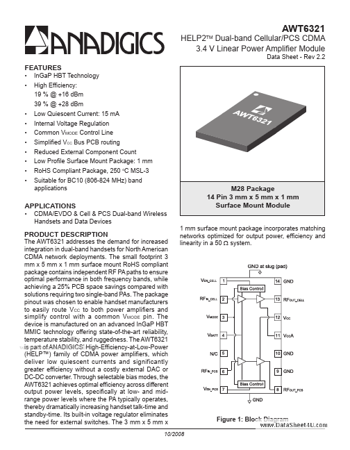
Figure 1: Block Diagram
10/2008
Figure 2: Pinout Table 1: Pin Description
PIN 1 2 3 4 5 6 7 NAME VEN_CELL RFIN_CELL VMODE VBATT N/C RFIN_PCS VEN_PCS RFOUT_PCS GND GND VCCA VCC DESCRIPTION
Enable Voltage for Cell Band RF Input for Cell Band Mode Control Voltage for Cell and PCS Bands Battery Voltage No Connection RF Input for PCS Band Enable Voltage for PCS Band RF Output for PCS Band Ground Ground Battery Voltage A Supply...