AT49BV8011
AT49BV8011 is 8-megabit (512K x 16/1M x 8) 3-volt Only Flash Memory manufactured by Atmel.
Features
- Single Supply for Read and Write: 2.7V to 3.3V (BV), 3.0V to 3.3V (LV)
- Access Time
- 90 ns
- Sector Erase Architecture
Fourteen 32K Word (64K Byte) Sectors with Individual Write Lockout Two 16K Word (32K Byte) Sectors with Individual Write Lockout Two 8K Word (16K Byte) Sectors with Individual Write Lockout Four 4K Word (8K Byte) Sectors with Individual Write Lockout Fast Word Program Time
- 20 µs Fast Sector Erase Time
- 200 ms Dual Plane Organization, Permitting Concurrent Read while Program/Erase Memory Plane A: Four 4K Word, Two 8K Word and Two 16K Word Sectors Memory Plane B: Fourteen 32K Word Sectors Erase Suspend Capability
- Supports Reading/Programming Data from Any Sector by Suspending Erase of Any Different Sector Low-power Operation
- 25 m A Active
- 10 µA Standby Data Polling, Toggle Bit, Ready/Busy for End of Program Detection Optional VPP Pin for Fast Programming RESET Input for Device Initialization Sector Program Unlock mand TSOP and CBGA Package Options Top or Bottom Boot Block Configuration Available
- -
- -
- -
- -
- -
- 8-megabit (512K x 16/1M x 8) 3-volt Only Flash Memory AT49BV8011 AT49BV8011T AT49LV8011 AT49LV8011T
Description
The AT49BV/LV8011(T) is a 2.7- to 3.3-volt 8-megabit Flash memory organized as 524,288 words of 16 bits each or 1,048,576 bytes of 8 bits each. The x16 data appears on I/O0
- I/O15; the x8 data appears on I/O0
- I/O7. The memory is divided into 22 sectors for erase operations. The device is offered in 48-pin TSOP and 48-ball CBGA packages. The device has CE, and OE control signals to avoid any bus
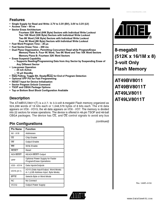
Pin Configurations
Pin Name
A0
- A18 CE OE WE RESET RDY/BUSY VPP I/O0
- I/O14 I/O15 (A-1) BYTE NC VCCQ
(continued)
Function
Addresses Chip Enable Output Enable Write Enable Reset READY/BUSY Output Optional Power Supply for Faster Program/Erase Operations Data Inputs/Outputs I/O15 (Data Input/Output, Word Mode) A-1 (LSB Address Input, Byte Mode) Selects Byte or Word Mode No Connect Output Power Supply
Rev....