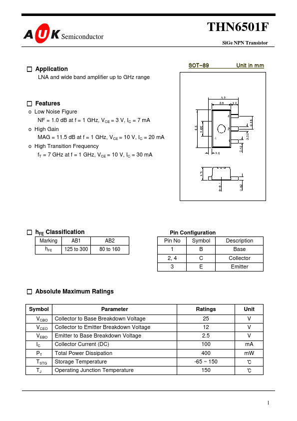
Click to expand full text
Semiconductor
□ Application
LNA and wide band amplifier up to GHz range
□ Features
o Low Noise Figure NF = 1.0 dB at f = 1 GHz, VCE = 3 V, IC = 7 mA
o High Gain MAG = 11.5 dB at f = 1 GHz, VCE = 10 V, IC = 20 mA
o High Transition Frequency fT = 7 GHz at f = 1 GHz, VCE = 10 V, IC = 30 mA
THN6501F
SiGe NPN Transistor
SOT-89
Unit in mm
4
□ hFE Classification
Marking
AB1
hFE 125 to 300
AB2 80 to 160
Pin Configuration Pin No Symbol
1B 2, 4 C
3E
Description Base
Collector Emitter
□ Absolute Maximum Ratings
Symbol
Parameter
VCBO VCEO VEBO IC PT TSTG TJ
Collector to Base Breakdown Voltage Collector to Emitter Breakdown Voltage Emitter to Base Breakdown Voltage Collector Current (DC) Total Power Dissipation Storage Temperature Operating Junction Temperature
Ratings 25 12 2.