AFP2325S
AFP2325S is P-Channel Enhancement Mode MOSFET manufactured by Alfa-MOS.
- Part of the AFP2325S-Alfa comparator family.
- Part of the AFP2325S-Alfa comparator family.
Description
AFP2325S, P-Channel enhancement mode MOSFET, uses Advanced Trench Technology to provide excellent RDS(ON), low gate charge. These devices are particularly suited for low voltage power management, and low in-line power loss are needed in mercial industrial surface mount applications.
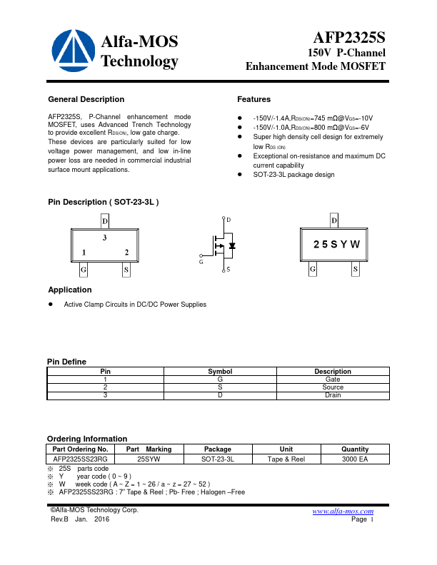
Pin Description
( SOT-23-3L )
150V P-Channel Enhancement Mode MOSFET
Features
-150V/-1.4A,RDS(ON)=745 mΩ@VGS=-10V -150V/-1.0A,RDS(ON)=800 mΩ@VGS=-6V Super high density cell design for extremely low RDS (ON) Exceptional on-resistance and maximum DC current capability SOT-23-3L package design
Application
Active Clamp Circuits in DC/DC Power Supplies
Pin Define
Pin 1 2 3
Symbol G S D
Description
Gate Source Drain
Ordering Information
Part Ordering No.
Part Marking
Package
AFP2325SS23RG
25SYW
SOT-23-3L
※ 25S parts code ※ Y year code ( 0 ~ 9 ) ※ W week code ( A ~ Z = 1 ~ 26 / a ~ z = 27 ~ 52 )
※ AFP2325SS23RG : 7” Tape & Reel ; Pb- Free ; Halogen
- Free
©Alfa-MOS Technology Corp. Rev.B Jan. 2016
Unit Tape & Reel
Quantity 3000 EA
.alfa-mos.
Page 1
Alfa-MOS
Technology
150V P-Channel Enhancement Mode MOSFET
Absolute Maximum Ratings
(TA=25℃ Unless otherwise noted)
Drain-Source Voltage Gate
- Source Voltage
Parameter
Continuous Drain Current(TJ=150℃)
Pulsed Drain Current Continuous Source Current(Diode Conduction)
Power...