AS7C33128PFD32A
AS7C33128PFD32A is 3.3V 128K X 32/36 pipeline burst synchronous SRAM manufactured by Alliance Semiconductor Corporation.
Features
- Organization: 131,072 words × 32 or 36 bits
- Fast clock speeds to 166 MHz in LVTTL/LVCMOS
- Fast clock to data access: 3.5/3.8/4.0/5.0 ns
- Fast OE access time: 3.5/3.8/4.0/5.0 ns
- Fully synchronous register-to-register operation
- Single register “Flow-through” mode
- Dual-cycle deselect
- Single-cycle deselect also available (AS7C33128PFS32A/ .. AS7C33128PFS36A)
- Pentium®- patible architecture and timing
- Asynchronous output enable control
- Economical 100-pin TQFP package
- Byte write enables
- Multiple chip enables for easy expansion
- 3.3 core power supply
- 2.5V or 3.3V I/O operation with separate VDDQ
- 30 m W typical standby power in power down mode
- NTD™- pipeline architecture available (AS7C33128KNTD32A/ AS7C33128NTD36A)
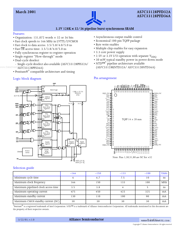
Logic block diagram
LBO CLK ADV ADSC ADSP A[16:0] 17 CLK CE CLR D CE Address register CLK D Q0 Burst logic Q1 17 Q
Pin arrangement
A6 A7 CE0 CE1 BWd BWc BWb BWa CE2 VDD VSS CLK GWE BWE OE ADSC ADSP ADV A8 A9 128K × 32/36 Memory array 100 99 98 97 96 95 94 93 92 91 90 89 88 87 86 85 84 83 82 81
GWE BWE BWd
DQd Q Byte write registers CLK D DQc Q Byte write registers CLK D DQb Q Byte write registers CLK D DQa Q Byte write registers CLK D Enable CE register CLK Power down D Enable Q delay register CLK Q
36/32
36/32
BWc
BWb
BWa CE0 CE1 CE2
OE FT DATA [35:0] DATA [31:0]
Note: Pins 1,30,51,80 are NC for ×32
Selection guide
- 166
- 150
- 133
- 100 Units
Minimum cycle time Maximum clock frequency Maximum pipelined clock access time Maximum operating current Maximum standby current Maximum CMOS standby current...