ASM5I23S09A
ASM5I23S09A is 3.3V SpreadTrak Zero Delay Buffer manufactured by Alliance Semiconductor.
- Part of the ASM5I23S05A comparator family.
- Part of the ASM5I23S05A comparator family.
Features
- -
- 10 MHz to 133- MHz operating range, patible with CPU and PCI bus frequencies. Zero input
- output propagation delay. Multiple low-skew outputs.
- -
..
- ASMP5P23S09A ASMP5P23S05A
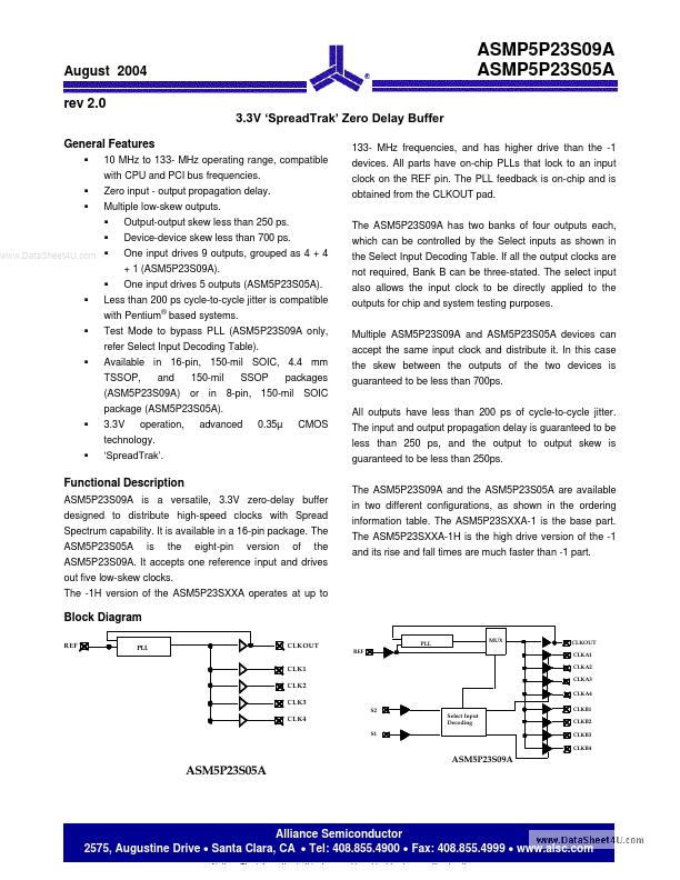
133- MHz frequencies, and has higher drive than the -1 devices. All parts have on-chip PLLs that lock to an input clock on the REF pin. The PLL feedback is on-chip and is obtained from the CLKOUT pad. The ASM5P23S09A has two banks of four outputs each, which can be controlled by the Select inputs as shown in the Select Input Decoding Table. If all the output clocks are not required, Bank B can be three-stated. The select input also allows the input clock to be directly applied to the outputs for chip and system testing purposes. Multiple ASM5P23S09A and ASM5P23S05A devices can accept the same input clock and distribute it. In this case the skew between the outputs of the two devices is guaranteed to be less than 700ps. All outputs have less than 200 ps of cycle-to-cycle jitter. 0.35µ CMOS The input and output propagation delay is guaranteed to be less than 250 ps, and the output to output skew is guaranteed to be less than 250ps. The ASM5P23S09A and the ASM5P23S05A are available in two different configurations, as shown in the ordering information table. The ASM5P23SXXA-1 is the base part. The ASM5P23SXXA-1H is the high drive version of the -1 and its rise and fall times are much faster than -1 part. packages
Output-output skew less than 250 ps. Device-device skew less than 700 ps. One input drives 9 outputs, grouped as 4 + 4 + 1 (ASM5P23S09A). One input drives 5 outputs (ASM5P23S05A).
- -
- -
Less than 200 ps cycle-to-cycle jitter is patible with Pentium ® based systems. Test Mode to bypass PLL (ASM5P23S09A only, refer Select Input Decoding Table). Available in 16-pin, 150-mil SOIC, 4.4 mm TSSOP, and 150-mil SSOP (ASM5P23S09A) or in 8-pin, 150-mil SOIC package (ASM5P23S05A).
- -
3.3V operation, advanced technology. ‘Spread Trak’.
Functional Description
ASM5P23S09A...