Datasheet Details
| Part number | AOD488 |
|---|---|
| Manufacturer | Alpha & Omega Semiconductors |
| File Size | 149.22 KB |
| Description | N-Channel MOSFET |
| Datasheet |
 AOD488 Datasheet AOD488 Datasheet
|
|
|
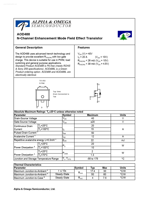
The AOD488 uses advanced trench technology and design to provide excellent R DS(ON) with low gate charge.
This device is suitable for use in PWM, load switching and general purpose applications.
Standard Product AOD488 is Pb-free (meets ROHS & Sony 259 specifications).
| Part number | AOD488 |
|---|---|
| Manufacturer | Alpha & Omega Semiconductors |
| File Size | 149.22 KB |
| Description | N-Channel MOSFET |
| Datasheet |
AOD488 Datasheet
|
|
|
|
Note: Below is a high-fidelity text extraction (approx. 800 characters) for AOD488. For precise diagrams, and layout, please refer to the original PDF.
www.DataSheet4U.com AOD488 N-Channel Enhancement Mode Field Effect Transistor General Description The AOD488 uses advanced trench technology and design to provide excelle...
| Part Number | Description |
|---|---|
| AOD480 | 30V N-Channel MOSFET |
| AOD482 | 100V N-Channel MOSFET |
| AOD484 | N-Channel MOSFET |
| AOD486A | 40V N-Channel MOSFET |
| AOD400 | N-Channel MOSFET |
| AOD402 | N-Channel MOSFET |
| AOD403 | 30V P-Channel MOSFET |
| AOD404 | N-Channel MOSFET |
| AOD405 | P-Channel MOSFET |
| AOD406 | N-Channel Enhancement Mode Field Effect Transistor |