Datasheet Details
| Part number | AON3820 |
|---|---|
| Manufacturer | Alpha & Omega Semiconductors |
| File Size | 328.97 KB |
| Description | Dual N-Channel MOSFET |
| Download | AON3820 Download (PDF) |
|
|
| Part number | AON3820 |
|---|---|
| Manufacturer | Alpha & Omega Semiconductors |
| File Size | 328.97 KB |
| Description | Dual N-Channel MOSFET |
| Download | AON3820 Download (PDF) |
|
|
|
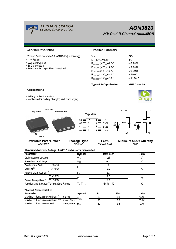
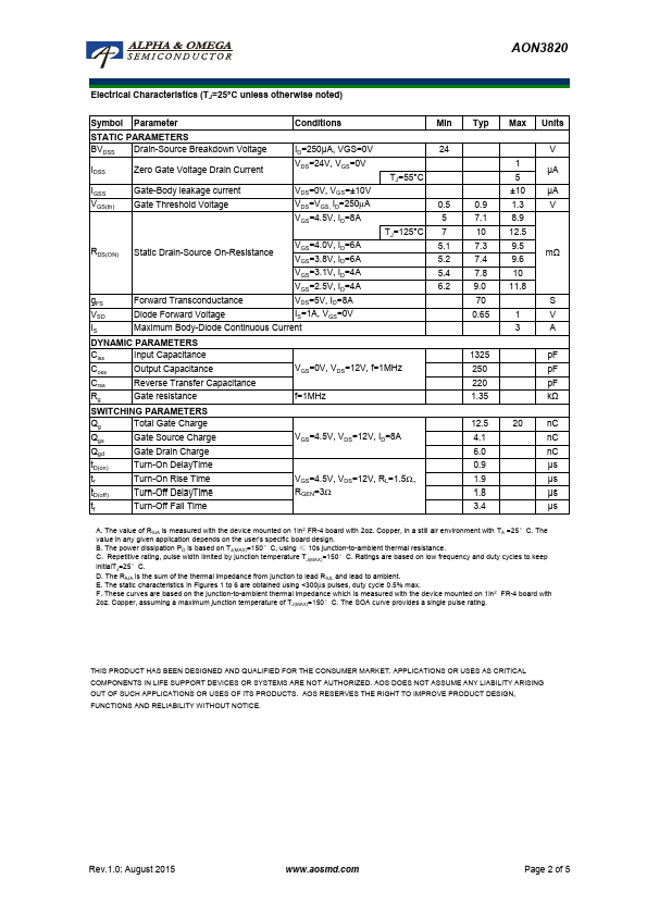
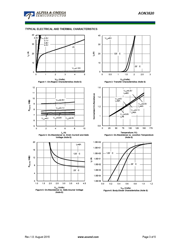
• Trench Power AlphaMOS (αMOS LV) technology • Low RDS(ON) • Low Gate Charge • ESD protection • RoHS and Halogen-Free Compliant Applications • Battery protection switch • Mobile device battery charging and discharging Product Summary VDS ID (at VGS=4.5V) RDS(ON) (at VGS=4.5V) RDS(ON) (at VGS=4.0V) RDS(ON) (at VGS=3.7V) RDS(ON) (at VGS=3.1V) RDS(ON) (at VGS=2.5V) Typical ESD protection 24V 8A < 8.9mΩ < 9.5mΩ < 9.6mΩ < 10mΩ < 11.8mΩ HBM Class 3A Top View DFN 3x3 Bottom View Top View D1 D2 Pin 1 Orderable Part Number AON3820 S2 1 G2 2 S1 3 G1 4 Package Type DFN 3x3 8 D1/D2 7 D1/D2 6 G1 D1/D2 G2 5 D1/D2 S1 S2 Form Tape & Reel Minimum Order Quantity 3000 Absolute Maximum Ratings TA=25°C unless otherwise noted Parameter Symbol Drain-Source Voltage VDS Gate-Source Voltage VGS Continuous Drain Current G TA=25°C TA=70°C ID Pulsed Drain Current C IDM TA=25°C Power Dissipation B TA=70°C PD Junction and Storage Temperature Range TJ, TSTG Maximum 24 ±12 8 6.2 32 2.0 1.3 -55 to 150 Units V V A W °C Thermal Characteristics Parameter Symbol Typ Maximum Junction-to-Ambient A Maximum Junction-to-Ambient A D t ≤ 10s Steady-State RθJA 50 70 Maximum Junction-to-Lead Steady-State RθJL 30 Max 60 85 35 Units °C/W °C/W °C/W Rev.1.0: August 2015 www.aosmd.com Page 1 of 5 AON3820 Electrical Characteristics (TJ=25°C unless otherwise noted) Symbol Parameter Conditions Min STATIC PARAMETERS BVDSS Drain-Source Breakdown Voltage ID=250µA, VGS=0V 24 IDSS Zero Gate Voltage Drain Current VDS=24V, VGS=0V TJ=55°C IGSS Gate-Body leakage current VDS=0V, VGS=±10V VGS(th) Gate Threshold Voltage VDS=VGS, ID=250µA 0.5 VGS=4.5V, ID=8A 5 TJ=125°C 7 RDS(ON) Static Drain-Source On-Resistance VGS=4.0V, ID=6A VGS=3.8V, ID=6A 5.1 5.2 VGS=3.1V, ID=4A 5.4 VGS=2.5V, ID=4A 6.2 gFS Forward Transconductance VDS=5V, ID=8A VSD Diode Forward Voltage IS=1A, VGS=0V IS Ma
AON3820 24V Dual N-Channel AlphaMOS General.
| Part Number | Description |
|---|---|
| AON3806 | Field Effect Transistor |
| AON3810 | 20V Dual N-Channel MOSFET |
| AON3812 | Field Effect Transistor |
| AON3814 | 20V Dual N-Channel MOSFET |
| AON3816 | 20V Dual N-Channel MOSFET |
| AON3818 | Dual N-Channel MOSFET |
| AON3402 | 20V N-Channel MOSFET |
| AON3406 | 30V N-Channel MOSFET |
| AON3408 | N-Channel MOSFET |
| AON3414 | 30V N-Channel MOSFET |