Datasheet Details
| Part number | AON3406 |
|---|---|
| Manufacturer | Alpha & Omega Semiconductors |
| File Size | 439.04 KB |
| Description | 30V N-Channel MOSFET |
| Datasheet |
 AON3406 Datasheet AON3406 Datasheet
|
|
|
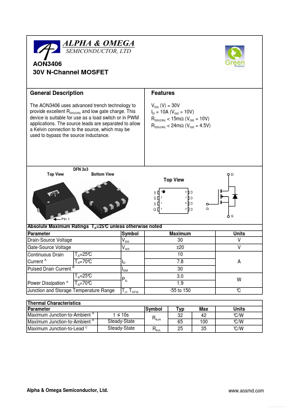
The AON3406 uses advanced trench technology to provide excellent RDS(ON) and low gate charge.
This device is suitable for use as a load switch or in PWM applications.
The source leads are separated to allow a Kelvin connection to the source, which may be used to bypass the source inductance.
| Part number | AON3406 |
|---|---|
| Manufacturer | Alpha & Omega Semiconductors |
| File Size | 439.04 KB |
| Description | 30V N-Channel MOSFET |
| Datasheet |
AON3406 Datasheet
|
|
|
|
| Part Number | Description | Manufacturer |
|---|---|---|
| AON2240 | N-Channel MOSFET | Kexin |
| AON2392 | N-Channel MOSFET | Kexin |
| AON6200L | 30V N-Channel MOSFET | Freescale |
| AON6405 | P-Channel MOSFET | VBsemi |
| AON6512 | N-Channel MOSFET | Kexin |
| Part Number | Description |
|---|---|
| AON3402 | 20V N-Channel MOSFET |
| AON3408 | N-Channel MOSFET |
| AON3414 | 30V N-Channel MOSFET |
| AON3601 | Field Effect Transistor |
| AON3611 | 30V Complementary MOSFET |
The following content is an automatically extracted verbatim text from the original manufacturer datasheet and is provided for reference purposes only.