Datasheet Details
| Part number | AON4413 |
|---|---|
| Manufacturer | Alpha & Omega Semiconductors |
| File Size | 169.18 KB |
| Description | Field Effect Transistor |
| Datasheet |
 AON4413 Datasheet AON4413 Datasheet
|
|
|
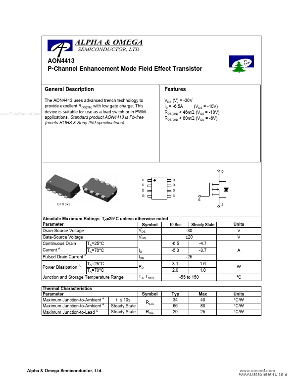
The AON4413 uses advanced trench technology to provide excellent RDS(ON) with low gate charge.
This www.DataSheet4U.com device is suitable for use as a load switch or in PWM applications.
Standard product AON4413 is Pb-free (meets ROHS & Sony 259 specifications).
| Part number | AON4413 |
|---|---|
| Manufacturer | Alpha & Omega Semiconductors |
| File Size | 169.18 KB |
| Description | Field Effect Transistor |
| Datasheet |
AON4413 Datasheet
|
|
|
|
| Part Number | Description | Manufacturer |
|---|---|---|
| AON2240 | N-Channel MOSFET | Kexin |
| AON2392 | N-Channel MOSFET | Kexin |
| AON6200L | 30V N-Channel MOSFET | Freescale |
| AON6405 | P-Channel MOSFET | VBsemi |
| AON6512 | N-Channel MOSFET | Kexin |
| Part Number | Description |
|---|---|
| AON4407 | 12V P-Channel MOSFET |
| AON4407L | P-Channel MOSFET |
| AON4420L | 30V N-Channel MOSFET |
| AON4421 | P-Channel Enhancement Mode Field Effect Transistor |
| AON4602 | Field Effect Transistor |
The following content is an automatically extracted verbatim text from the original manufacturer datasheet and is provided for reference purposes only.