Datasheet Details
| Part number | AONS520A70 |
|---|---|
| Manufacturer | Alpha & Omega Semiconductors |
| File Size | 689.44 KB |
| Description | N-Channel Power Transistor |
| Datasheet | AONS520A70-AlphaOmegaSemiconductors.pdf |
|
|
Overview: AONS520A70 700V, a MOS5 TM N-Channel Power Transistor General.
| Part number | AONS520A70 |
|---|---|
| Manufacturer | Alpha & Omega Semiconductors |
| File Size | 689.44 KB |
| Description | N-Channel Power Transistor |
| Datasheet | AONS520A70-AlphaOmegaSemiconductors.pdf |
|
|
|
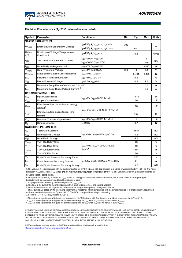
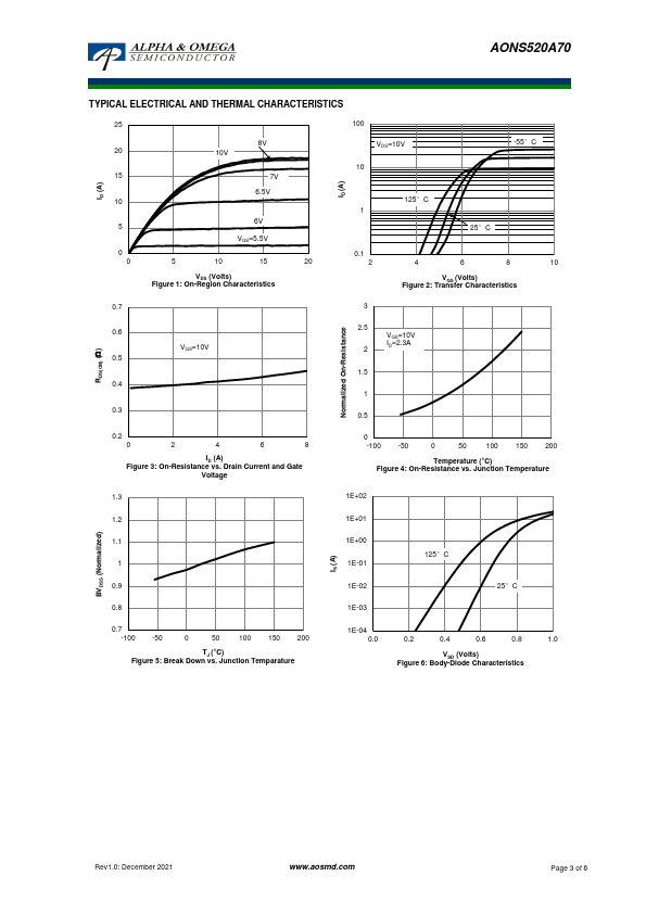
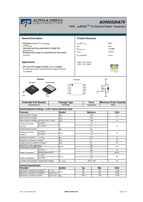
• Proprietary aMOS5TM technology • Low RDS(ON) • Optimized switching parameters for better EMI performance • Enhanced body diode for robustness and fast reverse recovery Applications • PFC and PWM stages (Flyback, LLC) of Adapter, PC Silverbox,Server,Gaming Power Supply,Industrial, TV,Lighting Product Summary VDS @ Tj,max IDM RDS(ON),max Qg,typ Eoss @ 400V 100% UIS Tested 100% Rg Tested 800V 44A < 0.52Ω 16.5nC 2.5mJ DFN5x6F Top View Bottom View PIN1 PIN1 Top View S1 S2 S3 G4 8D 7D 6D 5D D G S Orderable Part Number AONS520A70 Package Type DFN5X6F Absolute Maximum Ratings TA=25°C unless otherwise noted Parameter Symbol Drain-Source Voltage VDS Gate-Source Voltage VGS Gate-Source Voltage (dynamic) AC( f>1Hz) Continuous Drain TC=25°C Current TC=100°C Pulsed Drain Current C Continuous Drain Current Avalanche Current C TA=25°C TA=70°C L=1mH Repetitive avalanche energy C Single pulsed avalanche energy G MOSFET dv/dt ruggedness Peak diode recovery dv/dt VGS ID IDM IDSM IAR EAR EAS dv/dt TC=25°C Power Dissipation B Derate above 25°C PD TA=25°C Power Dissipation A TA=70°C PDSM Junction and Storage Temperature Range TJ, TSTG Thermal Characteristics Parameter Maximum Junction-to-Ambient A Maximum Junction-to-Ambient A D Maximum Junction-to-Case t ≤ 10s Steady-State Steady-State Symbol RqJA RqJC Form Tape&Reel Minimum Order Quantity 3000 Maximum 700 ±20 ±30 11 7.1 44 1.8 1.4 2.5 3.1 30 100 20 166 1.3 4.2 2.7 -55 to 150 Units V V V A A A mJ mJ V/ns W W/°C W °C Typ Max 25 30 45 55 0.49 0.75 Units °C/W °C/W °C/W Rev 1.0: December 2021 www.aosmd.com Page 1 of 6 AONS520A70 Electrical Characteristics (TJ=25°C unless otherwise noted) Symbol Parameter Conditions Min Typ Max Units STATIC PARAMETERS BVDSS Drain-Source Breakdown Voltage ID=250μA, VGS=0V, TJ=25°C ID=250μA, VGS=0V, TJ=150°C BVDSS /∆TJ Breakdown Voltage Temperature Coefficient ID=250μA
Compare AONS520A70 distributor prices and check real-time stock availability from major suppliers. Prices and inventory may vary by region and order quantity.
| Part Number | Description |
|---|---|
| AONS18314 | 30V N-Channel MOSFET |
| AONS1R1A70 | N-Channel Power Transistor |
| AONS21113 | 20V P-Channel MOSFET |
| AONS21303C | 30V P-Channel MOSFET |
| AONS21307 | 30V P-Channel MOSFET |
| AONS21309C | 30V P-Channel MOSFET |
| AONS21357 | 30V P-Channel MOSFET |
| AONS30300 | 30V N-Channel MOSFET |
| AONS30302 | 30V N-Channel Transistor |
| AONS32100 | 25V N-Channel MOSFET |