Datasheet Details
| Part number | AOU405 |
|---|---|
| Manufacturer | Alpha & Omega Semiconductors |
| File Size | 140.50 KB |
| Description | P-Channel MOSFET |
| Datasheet |
 AOU405 Datasheet AOU405 Datasheet
|

|
|
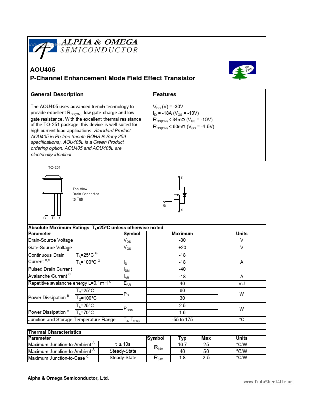
The AOU405 uses advanced trench technology to provide excellent RDS(ON), low gate charge and low gate resistance.
With the excellent thermal resistance of the TO-251 package, this device is well suited for high current load applications.
| Part number | AOU405 |
|---|---|
| Manufacturer | Alpha & Omega Semiconductors |
| File Size | 140.50 KB |
| Description | P-Channel MOSFET |
| Datasheet |
AOU405 Datasheet
|
|
|
|
| Part Number | Description | Manufacturer |
|---|---|---|
| AOU4N60 | N-Channel MOSFET | INCHANGE |
| AOU4S60 | N-Channel MOSFET | INCHANGE |
| AOU1N60 | N-Channel MOSFET | INCHANGE |
| AOU2N60 | N-Channel MOSFET | INCHANGE |
| AOU2N60A | 2A N-Channel MOSFET | INCHANGE |
| Part Number | Description |
|---|---|
| AOU400 | N-Channel MOSFET |
| AOU401 | P-Channel MOSFET |
| AOU402 | N-Channel MOSFET |
| AOU403 | P-Channel MOSFET |
| AOU404 | N-Channel MOSFET |
The following content is an automatically extracted verbatim text from the original manufacturer datasheet and is provided for reference purposes only.