AO4486 Overview
Description
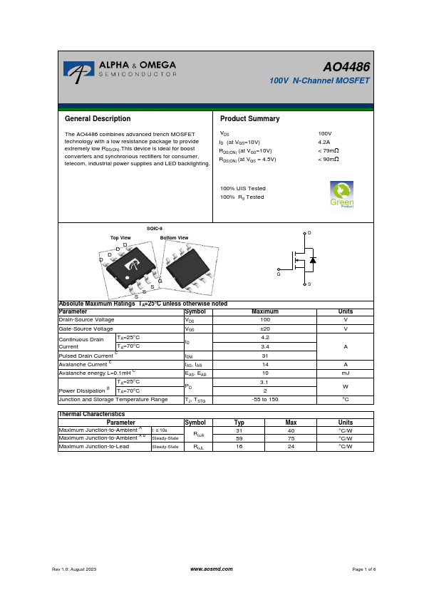
Product Summary The AO4486 combines advanced trench MOSFET technology with a low resistance package to provide extremely low RDS(ON).This device is ideal for boost converters and synchronous rectifiers for consumer, telecom, industrial power supplies and LED backlighting. VDS ID (at VGS=10V) RDS(ON) (at VGS=10V) RDS(ON) (at VGS = 4.5V) 100% UIS Tested 100% Rg Tested 100V 4.2A < 79mW < 90mW SOIC-8 D Top View Bottom View D D D D G G S S S S Parameter Symbol Maximum Drain-Source Voltage VDS 100 Gate-Source Voltage VGS ±20 Continuous Drain Current TA=25°C TA=70°C ID 4.2 3.4 Pulsed Drain Current C IDM 31 Avalanche Current C IAS, IAR 14 Avalanche energy L=0.1mH C EAS, EAR 10 TA=25°C Power Dissipation B TA=70°C PD 3.1 2 Junction and Storage Temperature Range TJ, TSTG -55 to 150 Parameter Symbol Typ Maximum Junction-to-Ambient A t ≤ 10s Maximum Junction-to-Ambient A D Steady-State RqJA 31 59 Maximum Junction-to-Lead Steady-State RqJL 16 Max 40 75 24 Units V V A A mJ W °C Units °C/W °C/W °C/W Rev 1.0: August 2023 Page 1 of 6 AO4486 Symbol Parameter Conditions Min Typ Max Units STATIC PARAMETERS BVDSS Drain-Source Breakdown Voltage ID=250mA, VGS=0V 100 V IDSS Zero Gate Voltage Drain Current VDS=100V, VGS=0V TJ=55°C 1 mA 5 IGSS Gate-Body leakage current VDS=0V, VGS= ±20V ±100 nA VGS(th) Gate Threshold Voltage VDS=VGS ID=250mA 1.6 2.2 2.7 V ID(ON) On state drain current VGS=10V, VDS=5V 31 A RDS(ON) Static Drain-Source On-Resistance VGS=10V, ID=3A TJ=125°C 62.5 79 mW 121 151 VGS=4.5V, ID=3A 68.5 90 mW gFS Forward Transconductance VDS=5V, ID=3A 20 S VSD Diode Forward Voltage IS=1A,VGS=0V 0.74 1 V IS Maximum Body-Diode Continuous Current 3.5 A DYNAMIC PARA.