AOU413
AOU413 is P-Channel MOSFET manufactured by Alpha & Omega Semiconductors.
Description
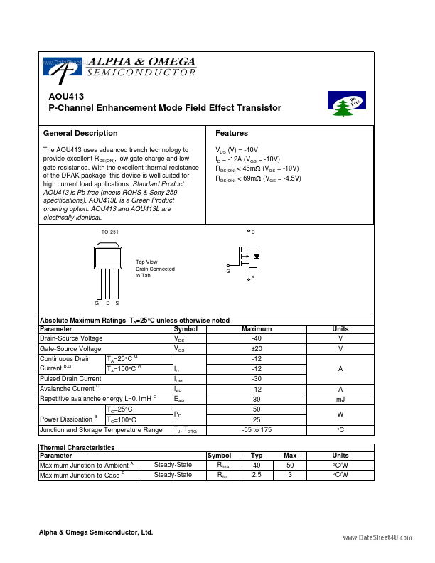
The AOU413 uses advanced trench technology to provide excellent RDS(ON), low gate charge and low gate resistance. With the excellent thermal resistance of the DPAK package, this device is well suited for high current load applications. Standard Product AOU413 is Pb-free (meets ROHS & Sony 259 specifications). AOU413L is a Green Product ordering option. AOU413 and AOU413L are electrically identical.
TO-251
Features
VDS (V) = -40V ID = -12A (VGS = -10V) RDS(ON) < 45mΩ (VGS = -10V) RDS(ON) < 69mΩ (VGS = -4.5V)
Top View Drain Connected to Tab
Absolute Maximum Ratings TA=25°C unless otherwise noted Parameter Symbol VDS Drain-Source Voltage VGS Gate-Source Voltage Continuous Drain Current B,G Pulsed Drain Current Avalanche Current C Repetitive avalanche energy L=0.1m H TC=25°C Power Dissipation B TC=100°C Junction and Storage Temperature Range Thermal Characteristics Parameter Maximum Junction-to-Ambient A Maximum Junction-to-Case C Steady-State Steady-State
Maximum -40 ±20 -12 -12 -30 -12 30 50 25 -55 to 175
Units V V A A m J W °C
TA=25°C
TA=100°C G
ID IDM IAR EAR PD TJ, TSTG
Symbol RθJA RθJL
Typ 40 2.5
Max 50 3
Units °C/W °C/W
Alpha & Omega Semiconductor, Ltd.
.. Electrical Characteristics (T J=25°C unless otherwise noted)
Symbol
Parameter
Conditions ID=-250µA, VGS=0V VDS=-32V, VGS=0V TJ=55°C VDS=0V, VGS=±20V VDS=VGS ID=-250µA VGS=-10V, VDS=-5V VGS=-10V, ID=-12A TJ=125°C VGS=-4.5V, I D=-8A VDS=-5V, ID=-12A
Min -40
Typ
Max
Units V
STATIC PARAMETERS BVDSS Drain-Source Breakdown Voltage IDSS IGSS VGS(th) ID(ON) RDS(ON) g FS VSD IS Zero Gate Voltage Drain Current Gate-Body leakage current Gate Threshold Voltage On state drain current Static Drain-Source On-Resistance Forward Transconductance
-1 -5 ±100 -1 -30 36 56 51 16 -0.75 -1 -12 657 45 70 69 -1.9 -3
µA n A V A mΩ mΩ S V A p F p F p F Ω n C n C n C n C ns ns ns ns ns n C
Diode Forward Voltage IS=-1A,VGS=0V Maximum Body-Diode Continuous Current
DYNAMIC PARAMETERS...