AOU417
AOU417 is P-Channel MOSFET manufactured by Alpha & Omega Semiconductors.
Description
The AOU417 uses advanced trench technology to provide excellent RDS(ON), and low gate charge. This device is suitable for use as a load switch or in PWM applications. Standard product AOU417 is Pbfree (meets ROHS & Sony 259 specifications).
Features
VDS (V) = -30V ID = -18A (VGS = -10V) RDS(ON) < 22mΩ (VGS = -10V) RDS(ON) < 40mΩ (VGS = -4.5V)
UIS TESTED! Rg,Ciss,Coss,Crss Tested
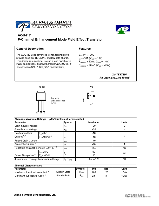
TO-251
Top View Drain Connected to Tab
Absolute Maximum Ratings TA=25°C unless otherwise noted Parameter Symbol VDS Drain-Source Voltage VGS Gate-Source Voltage Continuous Drain Current B,G Pulsed Drain Current Avalanche Current C Repetitive avalanche energy L=0.1m H TC=25°C Power Dissipation B TC=100°C Junction and Storage Temperature Range Thermal Characteristics Parameter Maximum Junction-to-Ambient A Maximum Junction-to-Case C Steady-State Steady-State
Maximum -30 ±20 -18 -18 -40 -18 16.2 50 25 -55 to 175
Units V V A A m J W °C
TA=25°C G TA=100°C G ID IDM IAR EAR PD TJ, TSTG
Symbol RθJA RθJL
Typ 105 2.5
Max 125 3
Units °C/W °C/W
Alpha & Omega Semiconductor, Ltd.
.aosmd.
.. Electrical Characteristics (T J=25°C unless otherwise noted)
Parameter Symbol STATIC PARAMETERS BVDSS Drain-Source Breakdown Voltage IDSS IGSS VGS(th) ID(ON) RDS(ON) g FS VSD IS ISM Zero Gate Voltage Drain Current Gate-Body leakage current Gate Threshold Voltage On state drain current Static Drain-Source On-Resistance
Conditions ID=-250µA, VGS=0V VDS=-30V, VGS=0V TJ=55°C VDS=0V, VGS=±20V VDS=VGS ID=-250µA VGS=-10V, VDS=-5V VGS=-10V, ID=-18A TJ=125°C VGS=-4.5V, ID=-10A VDS=-5V, ID=-18A
Min -30
Typ
Max
Units V
-1 -5 ±100 -1.4 -40 18 25 29 21 -0.7 -1 -1.2 -40 1573 1900 22 30 40 -2 -2.7
µA n A V A mΩ mΩ S V A A p F p F p F
Forward Transconductance
Diode Forward Voltage IS=-1A,VGS=0V Maximum Body-Diode Continuous Current Pulsed Body-Diode Current B
DYNAMIC PARAMETERS Ciss Input Capacitance Coss Crss Rg Output Capacitance Reverse Transfer Capacitance Gate resistance...