AOU401 Overview
Description
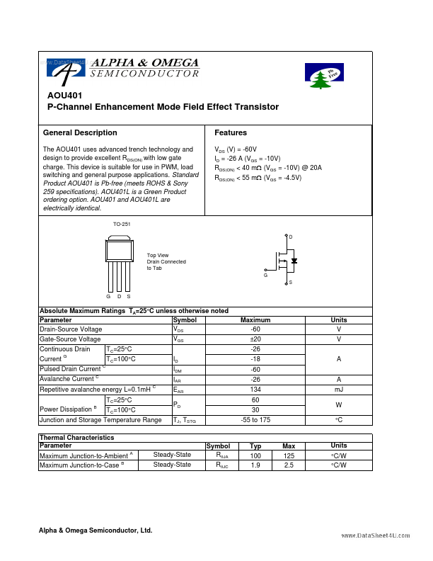
The AOU401 uses advanced trench technology and design to provide excellent RDS(ON) with low gate charge. This device is suitable for use in PWM, load switching and general purpose applications.
| Part | AOU401 |
|---|---|
| Description | P-Channel MOSFET |
| Category | MOSFET |
| Manufacturer | Alpha & Omega Semiconductors |
| Size | 106.30 KB |
The AOU401 uses advanced trench technology and design to provide excellent RDS(ON) with low gate charge. This device is suitable for use in PWM, load switching and general purpose applications.
| Seller | Inventory | Price Breaks | Buy |
|---|---|---|---|
| UnikeyIC | 400000 | 20+ : 0.6473 USD 40+ : 0.6365 USD 60+ : 0.6203 USD |
View Offer |
| Unikeyic (ICkey) | 400000 | 20+ : 0.6473 USD 40+ : 0.6365 USD 60+ : 0.6203 USD |
View Offer |
| Part Number | Manufacturer | Description |
|---|---|---|
| A2SHB | HAOHAI | N-Channel MOSFET |
| AP9563GH | Advanced Power Electronics Corp | P-CHANNEL ENHANCEMENT MODE POWER MOSFET |
| FCPF360N65S3R0L | onsemi | N-Channel MOSFET |