AOU402
AOU402 is N-Channel MOSFET manufactured by Alpha & Omega Semiconductors.
Description
The AOU402 uses advanced trench technology and design to provide excellent RDS(ON) with low gate charge. This device is suitable for use in PWM, load switching and general purpose applications. Standard Product AOU402 is Pb-free (meets ROHS & Sony 259 specifications). AOU402L is a Green Product ordering option. AOU402 and AOU402L are electrically identical.
TO-251 D
Features
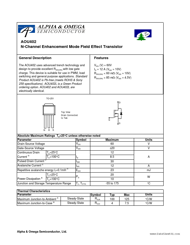
VDS (V) = 60V ID = 12 A (VGS = 10V) RDS(ON) < 60 mΩ (VGS = 10V) RDS(ON) < 85 mΩ (VGS = 4.5V)
Top View Drain Connected to Tab
Absolute Maximum Ratings TA=25°C unless otherwise noted Parameter Symbol VDS Drain-Source Voltage VGS Gate-Source Voltage Continuous Drain Current G Pulsed Drain Current Avalanche Current
Maximum 60 ±20 12 8.5 30 12 23 20 10 -55 to 175
Units V V A A m J W °C
TC=25°C TC=100°C ID IDM IAR EAR PD TJ, TSTG TC=25°C
Repetitive avalanche energy L=0.1m H Power Dissipation B TC=100°C
Junction and Storage Temperature Range Thermal Characteristics Parameter Maximum Junction-to-Ambient A Maximum Junction-to-Case B
Steady-State Steady-State
Symbol RθJA RθJC
Typ 100 4
Max 125 7.5
Units °C/W °C/W
Alpha & Omega Semiconductor, Ltd.
.. Electrical Characteristics (T J=25°C unless otherwise noted)
Parameter Symbol STATIC PARAMETERS BVDSS Drain-Source Breakdown Voltage IDSS IGSS VGS(th) ID(ON) RDS(ON) g FS VSD IS Zero Gate Voltage Drain Current Gate-Body leakage current Gate Threshold Voltage On state drain current Static Drain-Source On-Resistance
Conditions ID=10m A, VGS=0V VDS=48V, VGS=0V TJ=55°C VDS=0V, VGS=±20V VDS=VGS, ID=250µA VGS=10V, VDS=5V VGS=10V, ID=12A TJ=125°C VGS=4.5V, ID=6A VDS=5V, ID=12A
Min 60
Typ
Max
Units V
1 5 100 1 30 47 85 67 14 0.74 1 12 385 540 85 60 2.4 3
µA n A V A mΩ mΩ S V A p F p F p F
Forward Transconductance
Diode Forward Voltage IS=1A, VGS=0V Maximum Body-Diode Continuous Current
DYNAMIC PARAMETERS Ciss Input Capacitance Coss Crss Rg Output Capacitance Reverse Transfer Capacitance Gate resistance VGS=0V,...