FEATURES
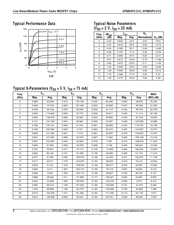
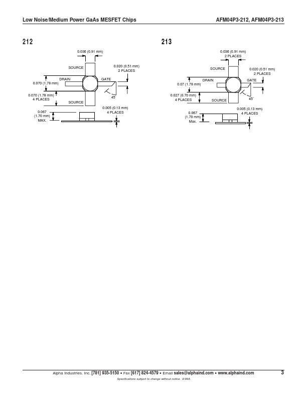
s Low Noise Figure, 0.6 dB @ 4 GHz s 20 dBm Output Power @ 18 GHz s High Associated Gain, 13 dB @ 4 GHz s High Power Added Efficiency, 25% s Broadband Operation, DC–26 GHz s Available in Tape and Reel Packaging Source 212 Gate Drain Source Gate Source Drain 213 Source DESCRIPTION
The AFM04P3 employs Ti/Pd/Au gate metallization and surface passivation to ensure a rugged, reliable part. ABSOLUTE MAXIMUM RATINGS
Characteristic Drain to Source Voltage (VDS) Gate to Source Voltage (VGS) Drain Current (IDS) Gate Current (IGS) Total Power Dissipation (PT) Storage Temperature (TST) Channel Temperature (TCH) Value 6V -4 V IDSS 1 mA 700 mW -65 to +150°C 175°C ELECTRICAL SPECIFICATIONS
at 25°C Parameter Saturated Drain Current (IDSS) Transconductance (gm) Pinch-Off Voltage (VP) Gate to Drain Breakdown Voltage (Vbgd) Noise Figure (NF) Associated Gain (GA) Output Power at 1 dB Compression (P1 dB) Gain at 1 dB Compression (G1 dB) Power Added Efficiency (ηadd) Test Conditions VDS = 2 V, VGS = 0 V VDS = 5 V, IDS = 1 mA IGD = -400 µA Min. Alpha Industries