FEATURES
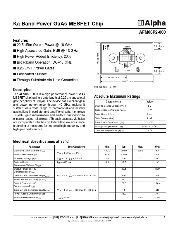
s 22.5 dBm Output Power @ 18 GHz s High Associated Gain, 9 dB @ 18 GHz s High Power Added Efficiency, 23% s Broadband Operation, DC–40 GHz s 0.25 µm Ti/Pd/Au Gates s Passivated Surface s Through-Substrate Via Hole Grounding 0.327 mm 0.655 mm Chip thickness = 0.1 mm. Drain 0.395 mm 0.110 mm Gate 0.110 mm DESCRIPTION
Through-substrate via holes are incorporated into the chip to facilitate low inductance grounding of the source for improved high frequency and high gain performance. ABSOLUTE MAXIMUM RATINGS
Characteristic Drain to Source Voltage (VDS) Gate to Source Voltage (VGS) Drain Current (IDS) Gate Current (IGS) Total Power Dissipation (PT) Storage Temperature (TST) Channel Temperature (TCH) Value 6V -4 V IDSS 1 mA 1.1 W -65 to +150°C 175°C ELECTRICAL SPECIFICATIONS
at 25°C Parameter Saturated Drain Current (IDSS) Transconductance (gm) Pinch-off Voltage (VP) Gate to Drain Breakdown Voltage (Vbgd) Output Power at 1 dB Compression (P1 dB) Gain at 1 dB Compression (G1 dB) Power... Alpha Industries