The following content is an automatically extracted verbatim text
from the original manufacturer datasheet and is provided for reference purposes only.
View original datasheet text
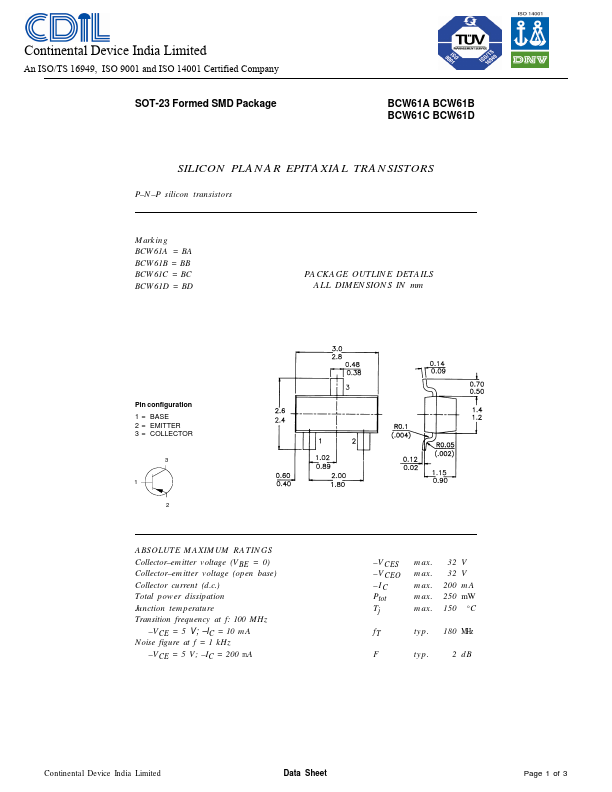
Continental Device India Limited
An ISO/TS 16949, ISO 9001 and ISO 14001 Certified Company
SOT-23 Formed SMD Package
BCW61A BCW61B BCW61C BCW61D
SILICON PLANAR EPITAXIAL TRANSISTORS
P–N–P silicon transistors
Marking BCW61A = BA BCW61B = BB BCW61C = BC BCW61D = BD
PACKAGE OUTLINE DETAILS ALL DIMENSIONS IN mm
Pin configuration 1 = BASE 2 = EMITTER 3 = COLLECTOR
3
1
2
ABSOLUTE MAXIMUM RATINGS Collector–emitter voltage (VBE = 0) Collector–emitter voltage (open base) Collector current (d.c.) Total power dissipation Junction temperature Transition frequency at f: 100 MHz
–VCE = 5 V; –IC = 10 mA Noise figure at f = 1 kHz
–VCE = 5 V; –IC = 200 mA
–VCES –VCEO –IC Ptot Tj
max. max. max. max. max.
32 V 32 V 200 mA 250 mW 150 °C
fT typ. 180 MHz
F typ.