Datasheet4U Logo Datasheet4U.com

MTP1406L3 - P-Channel Enhancement Mode Power MOSFET

Key Features

  • Simple Drive Requirement.
  • Low On-resistance.
  • Fast switching Characteristic.
  • Pb-free lead plating package BVDSS ID RDSON@VGS=-10V, ID=-4A RDSON@VGS=-10V, ID=-1.5A RDSON@VGS=-4.5V, ID=-2A -60V -4.8A 75mΩ (typ. ) 74mΩ (typ. ) 99mΩ (typ. ) Symbol MTP1406L3 Outline SOT-223 D S G:Gate D:Drain S:Source D G Absolute Maximum Ratings (Ta=25°C) Parameter Symbol Limits Unit Drain-Source Voltage Gate-Source Voltage Continuous Drain Current @ TA=25°C Continuous Drain C.

📥 Download Datasheet

Datasheet Details

Part number MTP1406L3
Manufacturer CYStech Electronics
File Size 329.26 KB
Description P-Channel Enhancement Mode Power MOSFET
Datasheet download datasheet MTP1406L3 Datasheet

Full PDF Text Transcription (Reference)

The following content is an automatically extracted verbatim text from the original manufacturer datasheet and is provided for reference purposes only.

View original datasheet text
CYStech Electronics Corp. P-Channel Enhancement Mode Power MOSFET Spec. No. : C733L3 Issued Date : 2012.02.14 Revised Date : 2012.03.09 Page No. : 1/8 MTP1406L3 Features • Simple Drive Requirement • Low On-resistance • Fast switching Characteristic • Pb-free lead plating package BVDSS ID RDSON@VGS=-10V, ID=-4A RDSON@VGS=-10V, ID=-1.5A RDSON@VGS=-4.5V, ID=-2A -60V -4.8A 75mΩ (typ.) 74mΩ (typ.) 99mΩ (typ.)
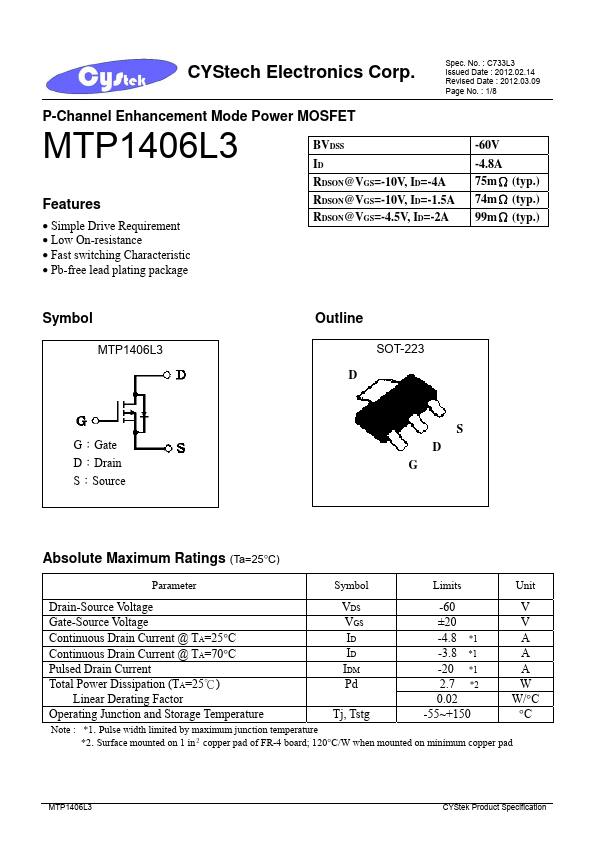
 Symbol MTP1406L3 Outline SOT-223 D S G:Gate D:Drain S:Source D G Absolute Maximum Ratings (Ta=25°C) Parameter Symbol Limits Unit Drain-Source Voltage Gate-Source Voltage Continuous Drain Current @ TA=25°C Continuous Drain Current @ TA=70°C Pulsed Drain Current Total Power Dissipation (TA=25℃) Linear Derating Factor Operating Junction and Storage Temperature Note : *1.