Datasheet Summary
CYStech Electronics Corp.
P-Channel Logic Level Enhancement Mode MOSFET
Spec. No. : C733M3 Issued Date : 2011.05.16 Revised Date : 2013.08.12 Page No. : 1/5
Features
- Single Drive Requirement
- Low On-resistance, RDS(ON)=90.8mΩ@VGS=-10V, ID=-4A
- Ultra High Speed Switching
- Pb-free lead plated package
BVDSS ID RDSON(MAX)
-60V -4A 90.8mΩ
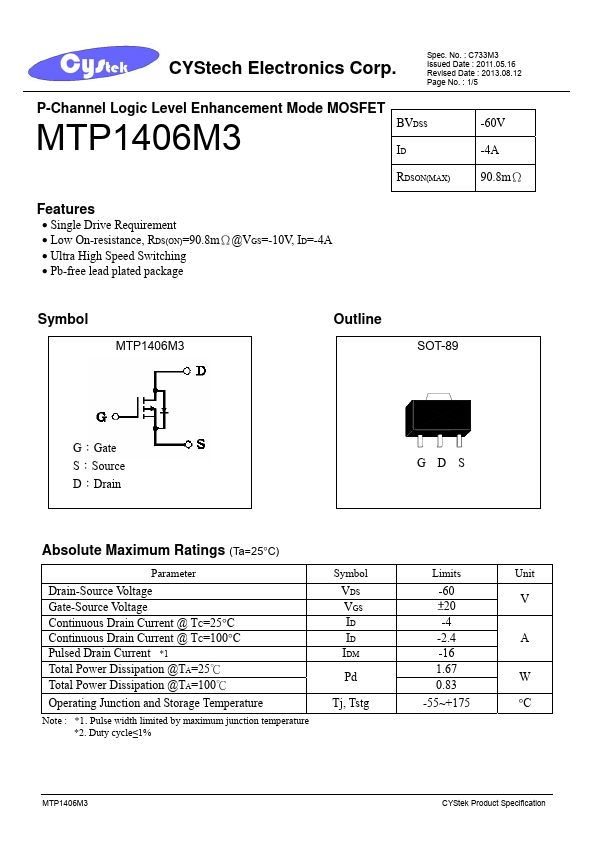
Symbol
Outline
SOT-89
G:Gate S:Source...