CYStech Electronics MTP2071M3
20V P-CHANNEL Enhancement Mode MOSFET
| Part No. | MTP2071M3 |
|---|---|
| Datasheet | MTP2071M3 Download |
| Manufacturer |  CYStech Electronics |
| Description | 20V P-CHANNEL Enhancement Mode MOSFET |
| Buy | Stock & Price |
FEATURES
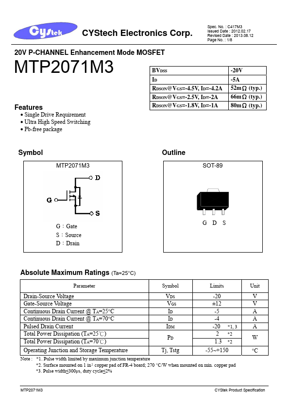
● Single Drive Requirement● Ultra High Speed Switching
● Pb-free package BVDSS ID RDSON@VGS=-4.5V, ID=-4.2A RDSON@VGS=-2.5V, ID=-2A RDSON@VGS=-1.8V, ID=-1A -20V -5A 52mΩ (typ.) 66mΩ (typ.) 80mΩ (typ.) Symbol MTP2071M3 Outline SOT-89 G:Gate S:Source D:Drain G D D S
ABSOLUTE MAXIMUM RATINGS
(Ta=25°C) Parameter Symbol Limits Unit Drain-Source Voltage Gate-Source Voltage Continuous Drain Current @ TA=25°C Continuous Drain Current @ TA=70°C Pulsed Drain Current Total Power Dissipation (TA=25℃) Total Power Dissipation (TA=70℃) Operating Junction and Storage Temperature Note : *1. Pulse width limited by maximum junction temperature VDS VGS ID ID IDM PD Tj, Tstg -20 ±12 -5 -4 -20 *1, 3 2 *2 1.3 *2 -55~+150 V V A A A W °C *2. Surface mounted on 1 in² copper pad of FR-4 board; 270 °C/W when mounted on min. copper pad *3. Pulse width≤300μs, duty cycle≤2% MTP2071M3 CYStek Product Specification CYStech Electronics Corp.THERMAL PERFORMANCE
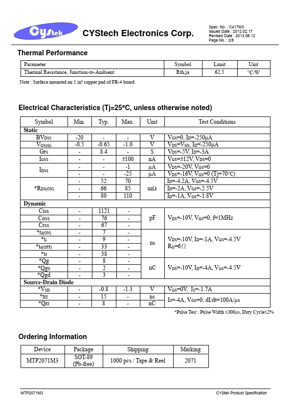
Parameter Thermal Resistance, Junction-to-Ambient Note : Surface mounted on 1 in² copper pad of FR-4 board.