CY29947
CY29947 is 1:9 Clock Distribution Buffer manufactured by Cypress.
2.5V or 3.3V, 200-MHz, 1:9 Clock Distribution Buffer
Features
- -
- -
- -
- -
- - 2.5V or 3.3V operation 200-MHz clock support LVCMOS-/LVTTL-patible inputs 9 clock outputs: drive up to 18 clock lines Synchronous Output Enable Output three-state control 250 ps max. output-to-output skew Pin patible with MPC947, MPC9447 Available in Industrial and mercial temp. range 32-pin TQFP package
Description
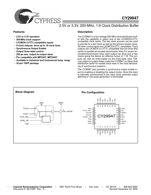
The CY29947 is a low-voltage 200-MHz clock distribution buffer with the capability to select one of two LVCMOS/LVTTL patible clock inputs. The two clock sources can be used to provide for a test clock as well as the primary system clock. All other control inputs are LVCMOS/LVTTL patible. The 9 outputs are LVCMOS or LVTTL patible and can drive 50Ω series or parallel terminated transmission lines.For series terminated transmission lines, each output can drive one or two traces giving the device an effective fanout of 1:18. The outputs can also be three-stated via the three-state input TS#. Low output-to-output skews make the CY29947 an ideal clock distribution buffer for nested clock trees in the most demanding of synchronous systems. The CY29947 also provides a synchronous output enable input for enabling or disabling the output clocks. Since this input is internally synchronized to the input clock, potential output glitching or runt pulse generation is eliminated.
Block Diagram
Pin Configuration
VDDC VDDC 27 VSS VSS VSS 25 24 23 22 21 20 19 18 17 Q0 Q1 28 Q2 26
VDD TCLK0 TCLK1 TCLK_SEL SYNC_OE TS# 0 1
VDDC
32 31 30 VSS TCLK_SEL TCLK0 TCLK1 SYNC_OE TS# VDD VSS 1 2 3 4 5 6 7 8 29 VSS Q3 VDDC Q4 VSS Q5 VDDC VSS
Q0-Q8
10 11 12 13 14 VDDC 15 Q6 16 VSS 9 VSS
Q8
..net Cypress Semiconductor Corporation
- 3901 North First Street
- San Jose
VDDC
- Document #: 38-07287 Rev.
- C
CA 95134
- 408-943-2600 Revised December 22, 2002
Q7
Pin Description[1]
Pin 3 4 2 11, 13, 15, 19, 21, 23, 26, 28, 30 5 6...