CY29949
CY29949 is 1:15 Clock Distribution Buffer manufactured by Cypress.
2.5V or 3.3V 200 MHz 1:15 Clock Distribution Buffer
Features
- -
- -
- -
- -
- -
- Description
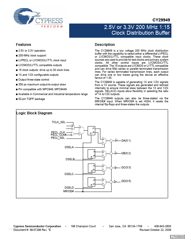
The CY29949 is a low voltage 200 MHz clock distribution buffer with the capability to select either a differential LVPECL or LVCMOS/LVTTL patible input clocks. These clock sources are used to provide for test clocks and primary system clocks. All other control inputs are LVCMOS/LVTTL patible. The 15 outputs are LVCMOS or LVTTL patible and can drive 50Ω series or parallel terminated transmission lines. For series terminated transmission lines, each output can drive one or two traces giving the device an effective fanout of 1:30. The CY29949 is capable of generating 1X and 1/2X signals from a 1X source. These signals are generated and retimed internally to ensure minimal skew between the 1X and 1/2X signals. SEL(A:D) inputs allow flexibility in selecting the ratio of 1X to1/2X outputs. The CY29949 outputs can also be three-stated via the MR/OE# input. When MR/OE# is set HIGH, it resets the internal flip-flops and three-states the outputs.
2.5V or 3.3V operation 200-MHz clock support LVPECL or LVCMOS/LVTTL clock input LVCMOS/LVTTL patible outputs 15 clock outputs: drive up to 30 clock lines 1X and 1/2X configurable outputs Output three-state control 350 ps maximum output-to-output skew Pin patible with MPC949, MPC9449 Available in mercial and Industrial temperature range 52-pin TQFP package
Logic Block Diagram
TCLK_SEL
0 1 0 1 R 1 2
PECL_CLK PECL_CLK# PECL_SEL DSELA
0 1
QA(0:1)
1 R 2
0 1
QB(0:2)
DSELB
1 R 2
0 1
QC(0:3)
DSELC
1 R 2 0 1 6
QD(0:5)
DSELD MR/OE#
..net
Cypress Semiconductor Corporation Document #: 38-07289 Rev.
-...