CY7C1007
Overview
- High speed - tAA = 12 ns
- CMOS for optimum speed/power
- Low active power - 825 mW
- Low standby power - 275 mW
- 2.0V data retention (optional) - 100 µW
- Automatic power-down when deselected
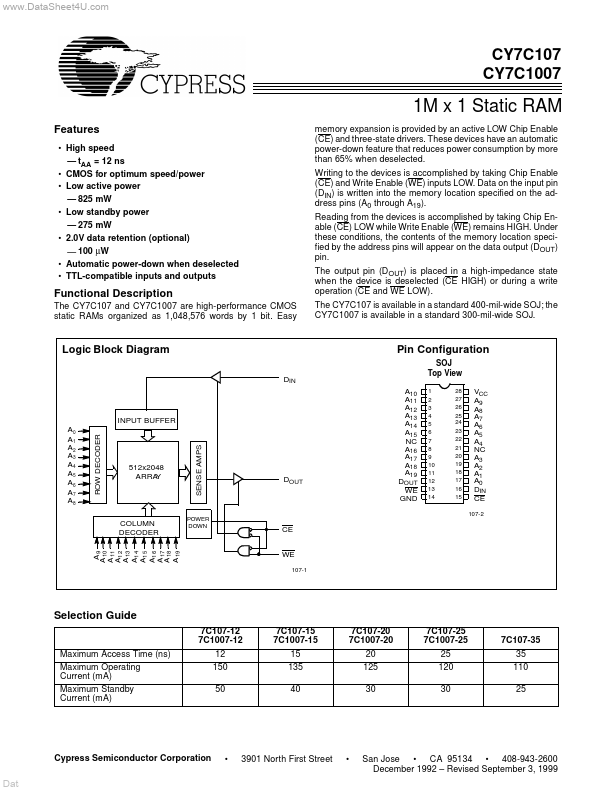
- TTL-compatible inputs and outputs memory expansion is provided by an active LOW Chip Enable (CE) and three-state drivers. These devices have an automatic power-down feature that reduces power consumption by more than 65% when deselected. Writing to the devices is accomplished by taking Chip Enable (CE) and Write Enable (WE) inputs LOW. Data on the input pin (DIN) is written into the memory location specified on the address pins (A0 through A19). Reading from the devices is accomplished by taking Chip Enable (CE) LOW while Write Enable (WE) remains HIGH. Under these conditions, the contents of the memory location specified by the address pins will appear on the data output (DOUT) pin. The output pin (D OUT) is placed in a high-impedance state when the device is deselected (CE HIGH) or during a write operation (CE and WE LOW). The CY7C107 is available in a standard 400-mil-wide SOJ; the CY7C1007 is available in a standard 300-mil-wide SOJ. Functional Description The CY7C107 and CY7C1007 are high-performance CMOS static RAMs organized as 1,048,576 words by 1 bit. Easy Logic Block Diagram DIN