CY7C1049DV33
CY7C1049DV33 is 4-Mbit (512K x 8) Static RAM manufactured by Cypress.
4-Mbit (512K x 8) Static RAM
Features
- -
Functional Description
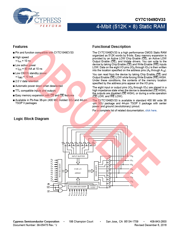
The CY7C1049DV33 is a high performance CMOS Static RAM organized as 512K words by 8-bits. Easy memory expansion is provided by an Active LOW Chip Enable (CE), an Active LOW Output Enable (OE), and tri-state drivers. You can write to the device by taking Chip Enable (CE) and Write Enable (WE) inputs LOW. Data on the eight IO pins (IO0 through IO7) is then written into the location specified on the address pins (A0 through A18). You can read from the device by taking Chip Enable (CE) and Output Enable (OE) LOW while forcing Write Enable (WE) HIGH. Under these conditions, the contents of the memory location specified by the address pins appear on the IO pins. The eight input or output pins (IO0 through IO7) are placed in a high impedance state when the device is deselected (CE HIGH), the outputs are disabled (OE HIGH), or during a write operation (CE LOW, and WE LOW). The CY7C1049DV33 is available in standard 400 Mil wide 36 -pin SOJ package and 44-pin TSOP II package with center power and ground (revolutionary) pinout. Refer to the Cypress application note AN1064, SRAM System Guidelines for best practice remendations.
Pin and function patible with CY7C1049CV33 High speed
- t AA = 10 ns Low active power
- ICC = 90 m A @ 10 ns (Industrial) Low CMOS standby power
- ISB2 = 10 m A 2.0V data retention Automatic power down when deselected TTL patible inputs and outputs Easy memory expansion with CE and OE Features
Available in Pb-free 36-pin (400 Mil) Molded SOJ and 44-pin TSOP II packages
- ..
- -
- -
- -
Logic Block Diagram
INPUT BUFFER A0 A1 A2 A3 A4 A5 A6 A7 A8 A9 A10 CE WE OE
IO0 IO1
ROW DECODER
512K x 8 ARRAY
SENSE AMPS
IO2 IO3 IO4 IO5 IO6
COLUMN DECODER
POWER DOWN
IO7
A11 A12 A13 A14 A15 A16 A17 A18
Cypress Semiconductor Corporation Document Number: 38-05475 Rev.
- D
- 198 Champion Court
- San Jose, CA 95134-1709
- 408-943-2600 Revised July 23,...