Datasheet4U Logo Datasheet4U.com

CY7C1381KVE33 - 18-Mbit Flow-Through SRAM

Download the CY7C1381KVE33 datasheet PDF. This datasheet also covers the CY7C1381KV33 variant, as both devices belong to the same 18-mbit flow-through sram family and are provided as variant models within a single manufacturer datasheet.

Key Features

  • Supports 133 MHz bus operations.
  • 512K × 36 and 1M × 18 common I/O.
  • 3.3 V core power supply (VDD).
  • 2.5 V or 3.3 V I/O supply (VDDQ).
  • Fast clock-to-output time.
  • 6.5 ns (133 MHz version).
  • Provides high performance 2-1-1-1 access rate.
  • User selectable burst counter supporting interleaved or linear burst sequences.
  • Separate processor and controller address strobes.
  • Synchronous self-timed write.
  • Asynchronous output enable.
  • CY7C1381KV.

📥 Download Datasheet

Note: The manufacturer provides a single datasheet file (CY7C1381KV33-CypressSemiconductor.pdf) that lists specifications for multiple related part numbers.

Full PDF Text Transcription (Reference)

The following content is an automatically extracted verbatim text from the original manufacturer datasheet and is provided for reference purposes only.

View original datasheet text
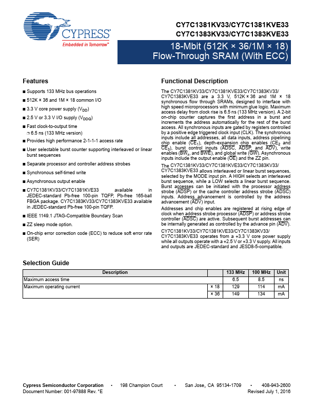
CY7C1381KV33/CY7C1381KVE33 CY7C1383KV33/CY7C1383KVE33 18-Mbit (512K × 36/1M × 18) Flow-Through SRAM (With ECC) 18-Mbit (512K × 36/1M × 18) Flow-Through SRAM (With ECC) Features ■ Supports 133 MHz bus operations ■ 512K × 36 and 1M × 18 common I/O ■ 3.3 V core power supply (VDD) ■ 2.5 V or 3.3 V I/O supply (VDDQ) ■ Fast clock-to-output time ❐ 6.5 ns (133 MHz version) ■ Provides high performance 2-1-1-1 access rate ■ User selectable burst counter supporting interleaved or linear burst sequences ■ Separate processor and controller address strobes ■ Synchronous self-timed write ■ Asynchronous output enable ■ CY7C1381KV33/CY7C1381KVE33 available in JEDEC-standard Pb-free 100-pin TQFP, Pb-free 165-ball FBGA package.