Datasheet4U Logo Datasheet4U.com

CY7C25682KV18 - 72-Mbit DDR II+ SRAM Two-Word Burst Architecture

Features

  • 72-Mbit density (4M × 18, 2M × 36).
  • 550 MHz clock for high bandwidth.
  • Two-word burst for reducing address bus frequency.
  • Double data rate (DDR) interfaces (data transferred at 1100 MHz) at 550 MHz.
  • Available in 2.5 clock cycle latency.
  • Two input clocks (K and K) for precise DDR timing.
  • SRAM uses rising edges only.
  • Echo Clocks (CQ and CQ) simplify data capture in high speed systems.
  • Data valid pin (QVLD) to indicate valid data on the output.
  • On-d.

📥 Download Datasheet

Full PDF Text Transcription (Reference)

The following content is an automatically extracted verbatim text from the original manufacturer datasheet and is provided for reference purposes only.

View original datasheet text
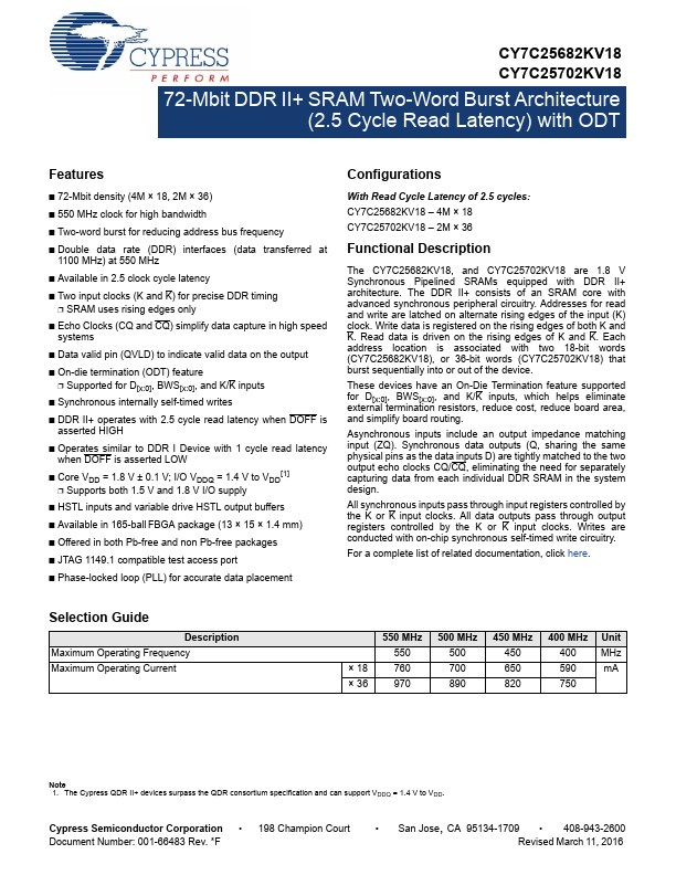
CY7C25682KV18 CY7C25702KV18 72-Mbit DDR II+ SRAM Two-Word Burst Architecture (2.5 Cycle Read Latency) with ODT 72-Mbit DDR II+ SRAM Two-Word Burst Architecture (2.5 Cycle Read Latency) with ODT Features ■ 72-Mbit density (4M × 18, 2M × 36) ■ 550 MHz clock for high bandwidth ■ Two-word burst for reducing address bus frequency ■ Double data rate (DDR) interfaces (data transferred at 1100 MHz) at 550 MHz ■ Available in 2.
Published: |