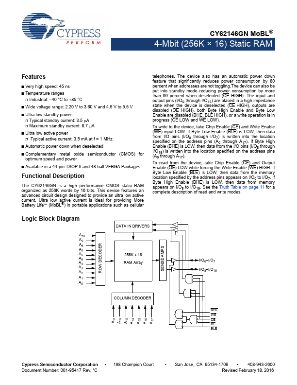
• Part: CY62146GN
  • Description: 4-Mbit (256K x 16) Static RAM
  • Manufacturer: Cypress
  • Size: 435.01 KB
Download CY62146GN Datasheet PDF
Cypress
CY62146GN
CY62146GN is 4-Mbit (256K x 16) Static RAM manufactured by Cypress.
CY62146GN Mo BL® 4-Mbit (256K × 16) Static RAM 4-Mbit (256K × 16) Static RAM Features - Very high speed: 45 ns - Temperature ranges - Industrial: - 40 °C to +85 °C - Wide voltage range: 2.20 V to 3.60 V and 4.5 V to 5.5 V - Ultra low standby power - Typical standby current: 3.5 A - Maximum standby current: 8.7 A - Ultra low active power - Typical active current: 3.5 m A at f = 1 MHz - Automatic power down when deselected - plementary metal oxide semiconductor (CMOS) for optimum speed and power - Available in a 44-pin TSOP II and 48-ball VFBGA Packages Functional Description The CY62146GN is a high performance CMOS static RAM organized as 256K words by 16 bits. This device Features an advanced circuit design designed to provide an ultra low active current. Ultra low active current is ideal for providing More Battery Life (Mo BL®) in portable applications such as cellular telephones. The device also has an automatic power down feature that significantly reduces power consumption by 80 percent when addresses are not toggling.The device can also be put into standby mode reducing power consumption by more than 99 percent when deselected (CE HIGH). The input and output pins (I/O0 through I/O15) are placed in a high impedance state when the device is deselected (CE HIGH), outputs are disabled (OE HIGH), both Byte High Enable and Byte Low Enable are disabled (BHE, BLE HIGH), or a write operation is in progress (CE LOW and WE LOW). To write to the device, take Chip Enable (CE) and Write Enable (WE) input LOW. If Byte Low Enable (BLE) is LOW, then data from I/O pins (I/O0 through I/O7) is written into the location specified on the address pins (A0 through A17). If Byte High Enable (BHE) is LOW, then data from the I/O pins (I/O8 through I/O15) is written into the location specified on the address pins (A0 through A17). To read from the device, take Chip Enable (CE) and Output Enable (OE) LOW while forcing the Write Enable (WE) HIGH. If Byte Low Enable (BLE) is LOW, then...