BTD882D3
BTD882D3 is NPN Transistor manufactured by Cystech Electonics Corp.
Features
- Low VCE(sat), VCE(sat)=0.25 V (typical), at IC / IB = 2A / 200m A
- Excellent current gain characteristics
- plementary to BTB772D3
- Pb-free package
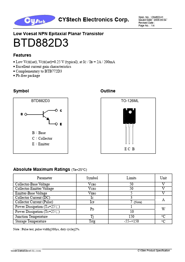
Symbol
Outline
TO-126ML
B:Base C:Collector E:Emitter EC B
Absolute Maximum Ratings (Ta=25°C)
Parameter Collector-Base Voltage Collector-Emitter Voltage Emitter-Base Voltage Collector Current (DC) Collector Current (Pulse) Power Dissipation (TA=25℃) Power Dissipation (TC=25℃) Junction Temperature Storage Temperature
Note : Pulse test, pulse width≤380µs, duty cycle≤2%.
Symbol VCBO VCEO VEBO IC ICP PD Tj Tstg
Limits 50 50 5 3 7 (Note) 1 10 150 -55~+150
Unit V V V A W °C °C
CYStek Product Specification
CYStech Electronics Corp.
Characteristics (Ta=25°C)
Symbol BVCBO BVCEO BVEBO ICBO IEBO
- VCE(sat)
- VBE(sat)
- h FE1
- h FE2
- h FE3 f T Cob Min. 50 50 5 150 180 100 Typ. 0.25 90 45 Max. 1 1 0.5 2 820 Unit V V V µA µA V V MHz p F
Spec. No. : C848D3-H .. Issued Date : 2005.05.04 Revised Date : Page No. : 2/4
Test Conditions IC=50µA, IE=0 IC=1m A, IB=0 IE=50µA, IC=0 VCB=40V, IE=0 VEB=5V, IC=0 IC=2A, IB=200m A IC=2A, IB=200m A VCE=2V, IC=20m A VCE=2V, IC=500m A VCE=2V, IC=1A VCE=5V, IC=100m A, f =100MHz VCB=10V, f=1MHz
- Pulse Test : Pulse Width ≤380µs, Duty Cycle≤2%
Classification Of h FE 2
Rank Range R 180~390 S 270~560 T 390~820
Characteristic Curves
Grounded Emitter Output Characteristics
140 Collector Current---IC(m A)
Grounded Emitter Output Characteristics
2.5m A 2m A 1.5m A 1m A 500u A IB=0u A
100 80 60 40 20 0 0 1 2 3 4
400u A 300u A 200u A 100u A IB=0u A
Collector Current---IC(m A)
500u...