74AUP1G09 Overview
Description
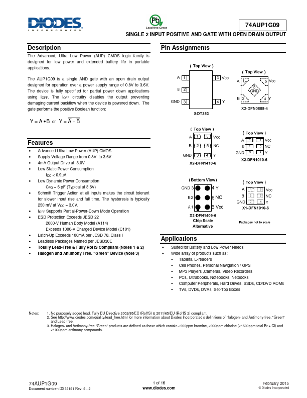
The Advanced, Ultra Low Power (AUP) CMOS logic family is designed for low power and extended battery life in portable applications. The AUP1G09 is a single AND gate with an open drain output designed for operation over a power supply range of 0.8V to 3.6V.
Key Features
- Advanced Ultra Low Power (AUP) CMOS
- Supply Voltage Range from 0.8V to 3.6V
- 4mA Output Drive at 3.0V
- Low Static Power Consumption ICC < 0.9µA
- Low Dynamic Power Consumption CPD = 6 pF (Typical at 3.6V)
- IOFF Supports Partial-Power-Down Mode Operation
- ESD Protection Exceeds JESD 22 2000-V Human Body Model (A114) Exceeds 1000-V Charged Device Model (C101)
- Latch-Up Exceeds 100mA per JESD 78, Class I
- Leadless Packages Named per JESD30E
- Totally Lead-Free & Fully RoHS Compliant (Notes 1 &