M53D1G1664A
M53D1G1664A is Mobile DDR SDRAM manufactured by Elite Semiconductor Microelectronics Technology.
ESMT
(Prliminary)
Mobile DDR SDRAM
16M x16 Bit x 4 Banks
Mobile DDR SDRAM
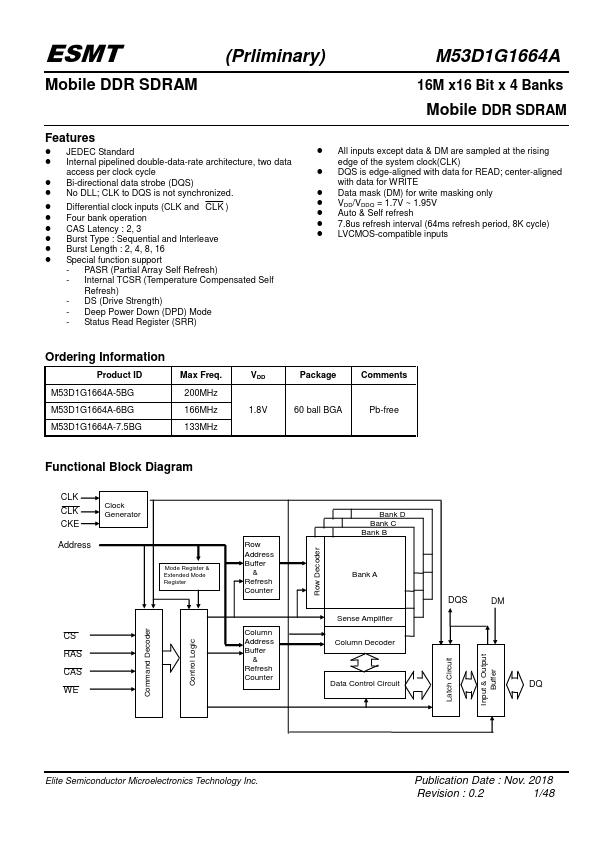
Features
- JEDEC Standard
- Internal pipelined double-data-rate architecture, two data access per clock cycle
- Bi-directional data strobe (DQS)
- No DLL; CLK to DQS is not synchronized.
- Differential clock inputs (CLK and CLK )
- Four bank operation
- CAS Latency : 2, 3
- Burst Type : Sequential and Interleave
- Burst Length : 2, 4, 8, 16
- Special function support
- PASR (Partial Array Self Refresh)
- Internal TCSR (Temperature pensated Self
Refresh)
- DS (Drive Strength)
- Deep Power Down (DPD) Mode
- Status Read Register (SRR)
- All inputs except data & DM are sampled at the rising edge of...