Datasheet4U Logo Datasheet4U.com

M56Z8G32256A - LPDDR4/LPDDR4X SDRAM

Description

Ball Name Type Function CK_t_A, CK_c_A, CK_t_B, CK_c_B Input CKE0_A, CKE1_A, CKE0_B, CKE1_B CS0_A, CS1_A, CS0_B, CS1_B CA[5:0]_A, CA[5:0]_B Input Input Input ODT_CA_A, ODT_CA_B Input DQ[15:0]_A, DQ[15:0]_B DQS[1:0]_t_A, DQS[1:0]_c_A, DQS[1:0]_t_B, DQS[1:0]_c_B Input / Output Input / Outp

📥 Download Datasheet

Datasheet preview – M56Z8G32256A

Datasheet Details

Part number M56Z8G32256A
Manufacturer ESMT
File Size 8.20 MB
Description LPDDR4/LPDDR4X SDRAM
Datasheet download datasheet M56Z8G32256A Datasheet
Additional preview pages of the M56Z8G32256A datasheet.
Other Datasheets by ESMT

Full PDF Text Transcription

Click to expand full text
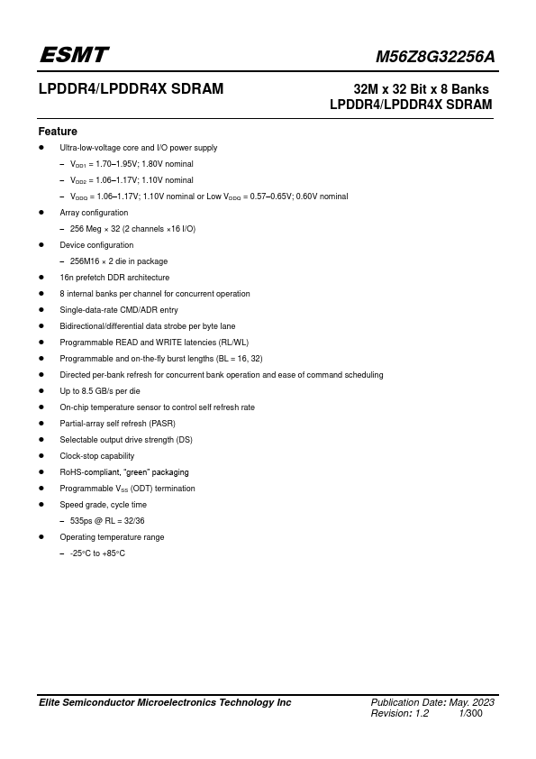
ESMT M56Z8G32256A LPDDR4/LPDDR4X SDRAM 32M x 32 Bit x 8 Banks LPDDR4/LPDDR4X SDRAM Feature  Ultra-low-voltage core and I/O power supply – VDD1 = 1.70–1.95V; 1.80V nominal – VDD2 = 1.06–1.17V; 1.10V nominal – VDDQ = 1.06–1.17V; 1.10V nominal or Low VDDQ = 0.57–0.65V; 0.60V nominal  Array configuration – 256 Meg × 32 (2 channels ×16 I/O)  Device configuration – 256M16 × 2 die in package  16n prefetch DDR architecture  8 internal banks per channel for concurrent operation  Single-data-rate CMD/ADR entry  Bidirectional/differential data strobe per byte lane  Programmable READ and WRITE latencies (RL/WL)  Programmable and on-the-fly burst lengths (BL = 16, 32)  Directed per-bank refresh for concurrent bank operation and ease of command scheduling  Up to 8.
Published: |