BUZ50A
BUZ50A is HIGH VOLTAGE POWER MOSFET manufactured by Unknown Manufacturer.
..
PRODUCT SPECIFICATIONS
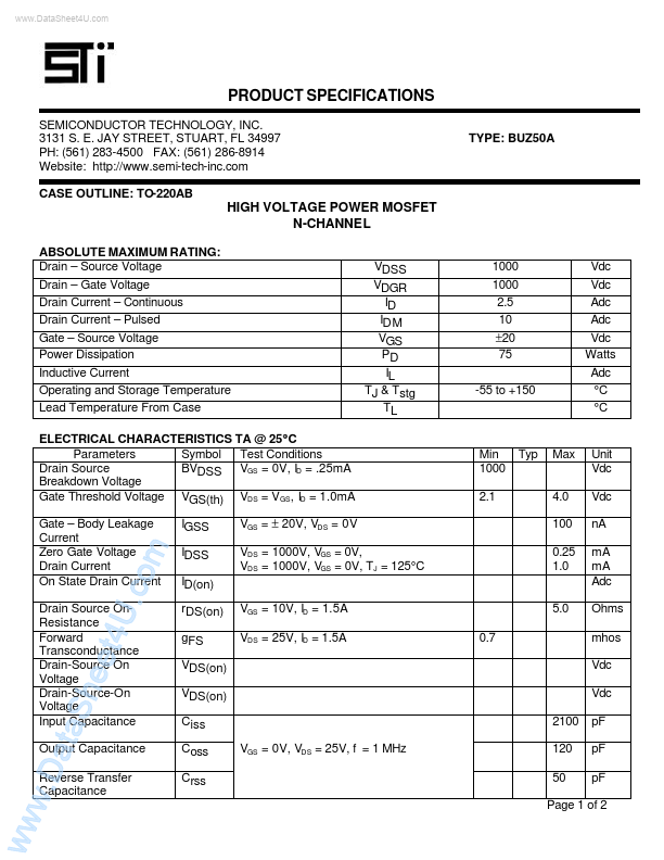
SEMICONDUCTOR TECHNOLOGY, INC. 3131 S. E. JAY STREET, STUART, FL 34997 PH: (561) 283-4500 FAX: (561) 286-8914 Website: http://.semi-tech-inc. CASE OUTLINE: TO-220AB TYPE: BUZ50A
HIGH VOLTAGE POWER MOSFET N-CHANNEL
ABSOLUTE MAXIMUM RATING: Drain
- Source Voltage Drain
- Gate Voltage Drain Current
- Continuous Drain Current
- Pulsed Gate
- Source Voltage Power Dissipation Inductive Current Operating and Storage Temperature Lead Temperature From Case ELECTRICAL CHARACTERISTICS TA @ 25° C Parameters Symbol Test Conditions Drain Source BVDSS VGS = 0V, ID = .25m A Breakdown Voltage Gate Threshold Voltage VGS(th) VDS = VGS, ID = 1.0m A Gate
- Body Leakage Current Zero Gate Voltage Drain Current On State Drain Current IGSS IDSS ID(on) r DS(on) g FS VDS(on) VDS(on) Ciss Coss Crss VGS = 0V, VDS = 25V, f = 1 MHz 2100 120 50 VGS = 10V, ID = 1.5A VDS = 25V, ID = 1.5A 0.7 5.0 VGS = ± 20V, VDS = 0V VDS = 1000V, VGS = 0V, VDS = 1000V, VGS = 0V, TJ = 125°C VDSS VDGR ID IDM VGS PD IL TJ & Tstg TL 1000 1000 2.5 10 ±20 75 -55 to +150 Vdc Vdc Adc Adc Vdc Watts Adc °C °C
Min 1000 2.1
Typ
Max
Unit Vdc Vdc n A m A m A Adc Ohms mhos Vdc Vdc p F p F p F
4.0 100 0.25 1.0
Drain Source On Resistance Forward Transconductance Drain-Source On Voltage Drain-Source-On Voltage Input Capacitance w.D a
Output Capacitance Reverse Transfer Capacitance ta S hee t4U .co m
Page 1 of 2 ww
..
TYPE: BUZ50A Drain Source Diode Characteristics Forward On Voltage IF = 5.0A, VGS = 0V Reverse Recovery Time Reverse Recovery Charge Total Gate Charge Gate
- Source Charge Gate
- Drain Charge IF = 2.5A di F /dt = 100A/µs, VGS = 0V VR = 100V Symbol VSD trr Qrr Qg Qgs Qgd Min Typ Max 1.3 Units Vdc ns µC n C n C n C
2000 15
Switching Characteristics Turn-On Time Turn-Off Time Delay Time (Turn On) Rise Time Delay Time (Turn Off) Fall Time VDD = 30V, ID = 2.0A VGS = 10V, RGS = 50Ω Rgen = 50Ω
Symbol ton toff td(on) tr td(off) tf
Min
Typ
Max
Units
45 60 140 80 ns ns ns ns ta S hee t4U .co...