EDD5116AFTA
EDD5116AFTA is 512M bits DDR SDRAM manufactured by Elpida Memory.
- Part of the EDD5108AFTA comparator family.
- Part of the EDD5108AFTA comparator family.
Description
The EDD5108AFTA and the EDD5116AFTA are 512M bits Double Data Rate (DDR) SDRAM organized as 16,777,216 words × 8 bits × 4 banks and 8,388,608 words × 16 bits × 4 banks, respectively. Read and write operations are performed at the cross points of the CK and the /CK. This high-speed data transfer is realized by the 2 bits prefetch-pipelined architecture. Data strobe (DQS) both for read and write are available for high speed and reliable data bus design. By setting extended mode register, the on-chip Delay Locked Loop (DLL) can be set enable or disable. It is packaged in standard 66-pin plastic TSOP (II).
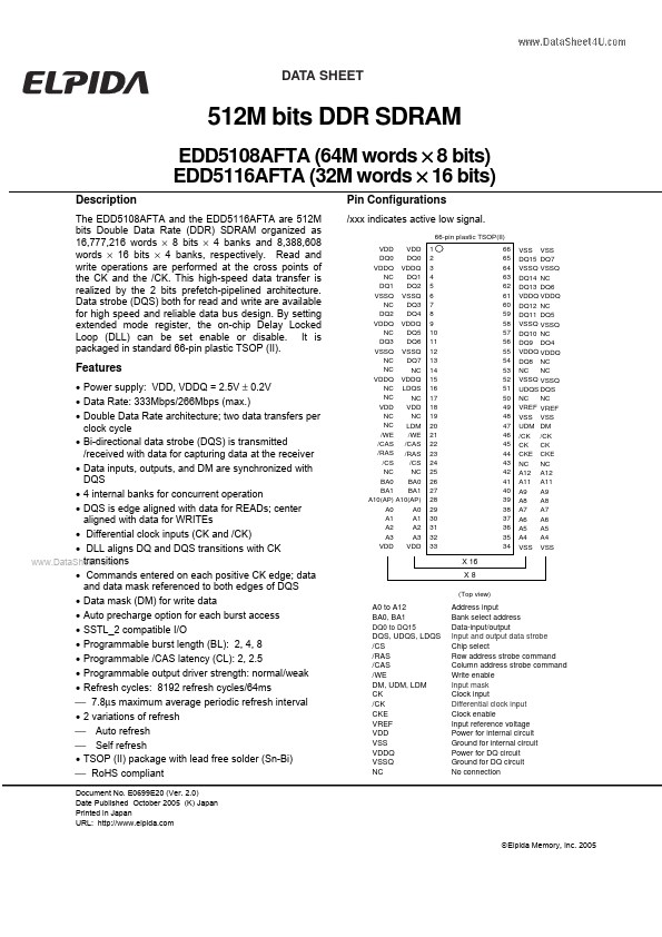
Pin Configurations
/xxx indicates active low signal.
66-pin plastic TSOP(II) VDD VDD DQ0 DQ0 VDDQ VDDQ NC DQ1 DQ1 DQ2 VSSQ VSSQ NC DQ3 DQ2 DQ4 VDDQ VDDQ NC DQ5 DQ3 DQ6 VSSQ VSSQ NC DQ7 NC NC VDDQ VDDQ NC LDQS NC NC VDD VDD NC NC NC LDM /WE /WE /CAS /CAS /RAS /RAS /CS /CS NC NC BA0 BA0 BA1 BA1 A10(AP) A10(AP) A0 A0 A1 A1 A2 A2 A3 A3 VDD VDD
Features
- Power supply: VDD, VDDQ = 2.5V ± 0.2V
- Data Rate: 333Mbps/266Mbps (max.)
- Double Data Rate architecture; two data transfers per clock cycle
- Bi-directional data strobe (DQS) is transmitted /received with data for capturing data at the receiver
- Data inputs, outputs, and DM are synchronized with DQS
- 4 internal banks for concurrent operation
- DQS is edge aligned with data for READs; center aligned with data for WRITEs
- Differential clock inputs (CK and /CK)
- DLL aligns DQ and DQS transitions with CK transitions ..
- mands entered on each positive CK edge; data and data mask referenced to both edges of DQS
- Data mask (DM) for write data
- Auto precharge option for each burst access
- SSTL_2 patible I/O
- Programmable burst length (BL): 2, 4, 8
- Programmable /CAS latency (CL): 2, 2.5
- Programmable output driver strength: normal/weak
- Refresh cycles: 8192 refresh cycles/64ms 7.8µs maximum average periodic refresh interval
- 2 variations of refresh Auto refresh Self refresh
- TSOP (II) package...