Datasheet4U Logo Datasheet4U.com

EM562161 - 128K x 16 Low Power SRAM

Description

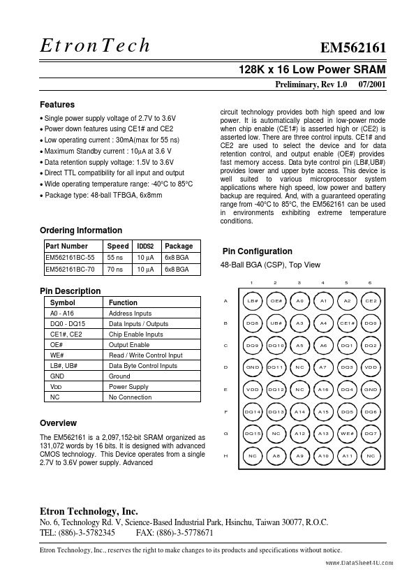
Symbol A0 - A16 DQ0 - DQ15 CE1#, CE2 OE# WE# LB#, UB# GND VDD NC Function Address Inputs Data Inputs / Outputs Chip Enable Inputs Output Enable Read / Write Control Input Data Byte Control Inputs Ground Power Supply No Connection A LB # O E# A0 A1 A2 CE 2 B DQ 8 UB # A3 A4 CE1 # DQ 0

Features

  • Single power supply voltage of 2.7V to 3.6V.
  • Power down features using CE1# and CE2.
  • Low operating current : 30mA(max for 55 ns).
  • Maximum Standby current : 10µA at 3.6 V.
  • Data retention supply voltage: 1.5V to 3.6V.
  • Direct TTL compatibility for all input and output.
  • Wide operating temperature range: -40°C to 85°C.
  • Package type: 48-ball TFBGA, 6x8mm EM562161 128K x 16 Low Power SRAM Preliminary, Rev 1.0 07/2001 circuit tec.

📥 Download Datasheet

Datasheet preview – EM562161

Datasheet Details

Part number EM562161
Manufacturer Etron Technology
File Size 140.13 KB
Description 128K x 16 Low Power SRAM
Datasheet download datasheet EM562161 Datasheet
Additional preview pages of the EM562161 datasheet.
Other Datasheets by Etron Technology

Full PDF Text Transcription

Click to expand full text
EtronTech Features • Single power supply voltage of 2.7V to 3.6V • Power down features using CE1# and CE2 • Low operating current : 30mA(max for 55 ns) • Maximum Standby current : 10µA at 3.6 V • Data retention supply voltage: 1.5V to 3.6V • Direct TTL compatibility for all input and output • Wide operating temperature range: -40°C to 85°C • Package type: 48-ball TFBGA, 6x8mm EM562161 128K x 16 Low Power SRAM Preliminary, Rev 1.0 07/2001 circuit technology provides both high speed and low power. It is automatically placed in low-power mode when chip enable (CE1#) is asserted high or (CE2) is asserted low. There are three control inputs. CE1# and CE2 are used to select the device and for data retention control, and output enable (OE#) provides fast memory access.
Published: |